


www.latticesemi.com 1 rd1026_01.9
November 2010 Reference Design RD1026
© 2010 Lattice Semiconductor Corp. All Lattice trademarks, registered trademarks, patents, and disclaimers are as listed at www.latticesemi.com/legal. All other brand
or product names are trademarks or registered trademarks of their respective holders. The specifications and information herein are subject to change without notice.
Introduction
The LatticeMico8™ is an 8-bit microcontroller optimized for Field Programmable Gate Arrays (FPGAs) and Pro-
grammable Logic Device architectures from Lattice. Combining a full 18-bit wide instruction set with 16 or 32 gen-
eral purpose registers, the LatticeMico8 is a flexible Verilog and VHDL reference design suitable for a wide variety
of markets, including communications, consumer, computer, medical, industrial and automotive. The core con-
sumes minimal device resources, less than 200 Look Up Tables (LUTs) in the smallest configuration, while main-
taining a broad feature set.
Features
• 8-bit Data Path
• 18-bit Wide Instructions
• Configurable 16 or 32 General Purpose Registers
• Scratch Pad Memory
• Input/Output is Performed Using Paged “Ports” (256 Ports/Page)
• Two/Three Cycles per Instruction
• Lattice UART Reference Design Peripheral
Functional Description
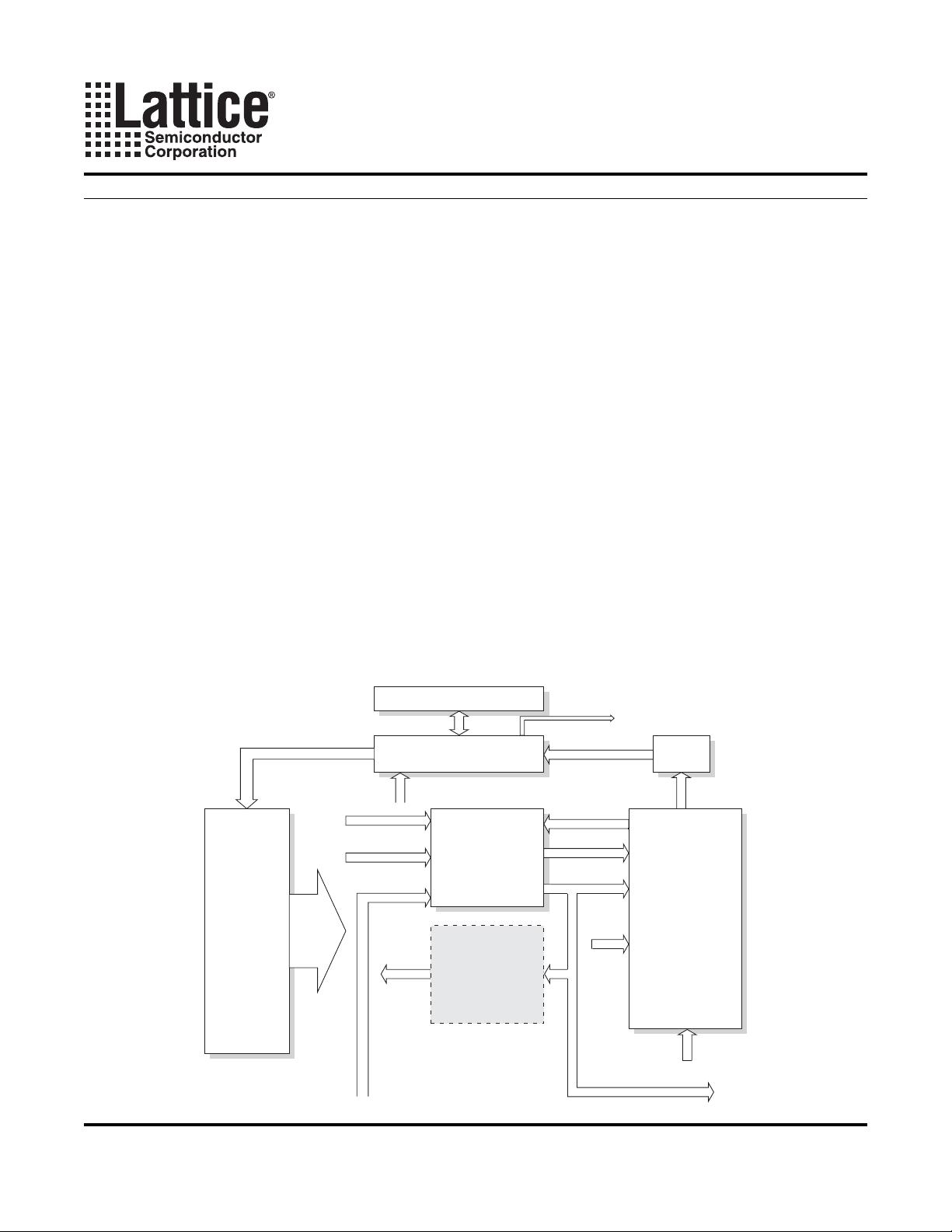
Figure 1 shows the LatticeMico8 microcontroller block diagram.
Figure 1. LatticeMico8 Microcontroller Block Diagram
Optional External
Scratch Pad
(up to 4G Bytes)
Register File
32 8-bit
Registers
Program
Memory
(EBR)
Program Flow Control and PC
16 Deep Call Stack
Interrupt Ack
value
ALU Op
From I/O Port
To I/O Port
op A
op B
Flags
CY, Z
rd
rb
instr
17:0
Interrupt
From Mem
Immediate
value
ALU
LatticeMico8 Microcontroller
User’s Guide

2
LatticeMico8 Microcontroller
Lattice Semiconductor User’s Guide
Exception Vectors
The LatticeMico8 provides two exception vectors. One vector address is used when the processor receives a reset,
the other when the processor receives an interrupt.
Address 0 should contain either an iret or unconditional branch instruction.
General Purpose Registers
The LatticeMico8 processor has either 16 or 32 8-bit general purpose registers. The registers are implemented
using a dual port distributed memory. The number of registers is configured prior to synthesizing the processor
core.
The LatticeMico8 opcode set permits the processor to access 32 registers. When the LatticeMico8 is configured
with 16 registers any opcode reference to R16 to R31 maps to R0 to R15 respectively.
Page Pointers
LatticeMico8 can directly access 256 memory locations. In order to increase the amount of memory it can address,
LatticeMico8 implements page pointers. General purpose registers R15, R14, and R13 have shadow registers. The
external address is the concatenation of R15, R14, and the address generated as a result of a direct/indirect mem-
ory opcode, where the output from these shadow registers becomes high-order address bits. This permits the
LatticeMico8 to address up to 4 GB of memory using 16M 256-byte pages.
The width of LatticeMico8 address is configurable from eight to 32 bits wide. When LatticeMico8 address bus size
is between 8 and 16 bits wide, the address bus presents the concatenation of R14 and 8 bits from the opcode
being executed. When LatticeMico8 address bus size is between 16 and 32 bits wide, the address bus presents the
concatenation of R15, R14, R13 and 8 bits from the opcode being executed. The high-order address bits controlled
by R15, R14, and R13 become active when the respective register is updated. The low-order 8 bits of the address
bus are valid during the second clock of the instruction and remain valid until the cycle terminates.
Scratch Pad RAM
LatticeMico8 provides an independent memory space that is designed to be used for scratch pad memory. The
size of this scratch pad can be configured from 32 bytes to 4G bytes. Page pointers are used when the scratch pad
size is larger than 256 bytes.
The scratch pad memory is always external. Direct addressing is used to access the first 32 bytes in the scratch
pad regardless of which scratch pad page is active. Indirect addressing can access all 256 bytes of the current
active scratch pad page.
Hardware (Circular) Call Stack
When a call instruction is executed, the address of the next instruction is pushed onto the call stack, a ret
(return) instruction will pop the stack and continue execution from the location at the top of the stack.
During an interrupt, the address of the next instruction is pushed onto the call stack. The processor jumps to the
interrupt vector at address 00000. Following an iret (return from interrupt) instruction the top-most address in the
call stack is popped, and execution resumes from the address retrieved from the stack.
The stack is implemented as a 16-entry (default) circular buffer and any program execution will continue from an
undefined location in case of a stack overflow or underflow. A synthesis parameter is available to adjust the size of
the call stack.
Address Function
0 External Int
1 Reset

3
LatticeMico8 Microcontroller
Lattice Semiconductor User’s Guide
Interrupt Handling
The microcontroller has one interrupt source, which is level-sensitive. The interrupt can be enabled or disabled by
software (cli = clear interrupt, sti = set interrupt). When an interrupt is received, the address of the next instruc-
tion is pushed into the call stack and the microcontroller continues execution from the interrupt vector (address 0).
The flags (carry and zero) are pushed onto the stack along with the return address. The interrupt ack line is
set high and the acknowledge line is held high for the entire duration of interrupt handling. Once the interrupt has
been acknowledged the interrupt line should be set to 0.
An iret instruction will pop the call stack and transfer control to the address on top of the stack. The flags (carry
and zero) are also popped from the call stack and restored. The interrupt acknowledge line is set to low.
The microcontroller cannot handle nested interrupts.
Input/Output
The LatticeMico8 external and scratch pad memory transactions occur synchronously to the LatticeMico8’s input
clock frequency. The external and scratch pad memories share a single address bus and an output data bus. The
input data for each memory is supplied on independent data buses.
The first 32 memory addresses can be accessed using either direct or indirect memory modes. The remaining 224
memory locations can be accessed using only indirect addressing modes.
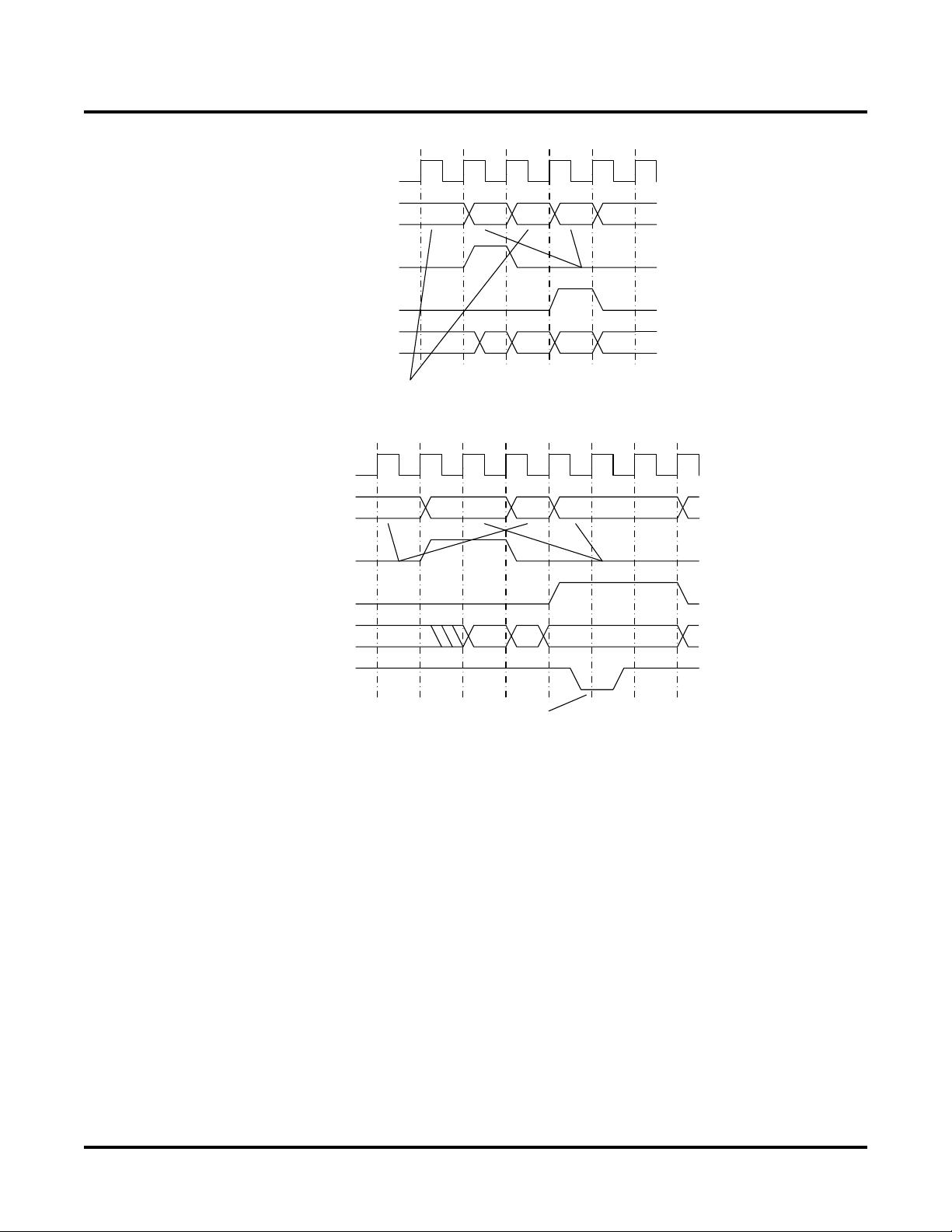
Figure 2 shows a v.2.4 memory transaction. The address and read/write strobe both appear in the second clock of
the processor's decode/execute cycle. The address and strobe only appear for a single clock pulse.
The scratch pad memory read and write strobes, ext_mem_rd/ext_mem_wr, go active as the result of the lsp, lspi,
ssp, and sspi opcodes.
The external port strobes, ext_io_rd/ext_io_wr, go active in response to the import, importi, export, exporti
opcodes.
The v.3.0 (and later) LatticeMico8 implementations modify the memory access times. Both the scratch pad and
external memory cycle times are increased by one clock cycle. Figure 3 shows an example of the v.3.0 bus cycle.
The v.3.0 bus cycle presents the address for a minimum of two clock cycles. Write data is also presented for a min-
imum of two clock cycles. Read data is captured at the rising clock edge of the third clock cycle.
The v.3.0 core also adds an external ready input. When driven LOW at the beginning of the third clock cycle a wait
state is inserted. Wait states continue to be asserted until the READY input is driven HIGH coincident to a rising
clock edge.
The transition to a three-clock cycle memory transaction in v.3.0 permits use of the FPGA’s EBR memory. The Lat-
tice EBR requires address be present for one clock prior to the data being read/written. The v.2.4 memory cycle
was incompatible with the EBR required behavior.
4
LatticeMico8 Microcontroller
Lattice Semiconductor User’s Guide
Figure 2. Version 2.4 Memory Transaction
Figure 3. Version 3.0 Bus Cycle Example
LatticeMico8 v.3.15 Enhancements
Version 3.15 of the LatticeMico8 adds some additional capabilities over earlier versions.
• Increased the number of shadow registers used for extended external addressing. Previously, R14 and R15 had
shadow registers. Version 3.15 offers three shadow registers for R13, R14 and R15.
• Increased Page pointers from 64K pages to 16M pages.
Increased the total addressable data memory to 4G Bytes.
LatticeMico8 v.3.1 Enhancements
Version 3.1 of the LatticeMico8 adds some additional capabilities over earlier versions.
• The interrupt handling is fixed. C and Z are correctly pushed to the stack
• This version also fixes asynchronous assertion of RESET
• All the branch instructions now have +/- 2K range
• Opcode decode 0x3c000 is now part of the reserved opcode for future use
CLK
Data[7:0]
MEM_RD/IO_RD
Port Address
MEM_WR/IO_WR
VAVA
RD WD
Fetch
Execute
CLK
Data[7:0]
MEM_RD/IO_RD
Port Address
MEM_WR/IO_WR
Ready
VA VA
RD WD
Fetch Execute
Insert
wait -state
5
LatticeMico8 Microcontroller
Lattice Semiconductor User’s Guide
LatticeMico8 v.3.0 Enhancements
Version 3.0 of the LatticeMico8 adds some additional capabilities over earlier versions.
• Addition of a READY signal for memory transactions
• 3 clock cycle memory transactions to support EBR and READY
• As described in the previous section the LatticeMico8 memory cycle times have increased by one clock. This
gives decode logic time to determine if a memory transaction needs to be lengthened to accommodate slow
memory and peripheral devices.
Increase in Instruction PROM Memory from 512 Lines to User-Defined Depth
The instruction memory size is now configurable using a passed HDL parameter. Sizes from 512 to 4096 lines of
code have been tested.
Unconditional Branch/Call Instructions Increased to +/- 2K Instruction Range
The increase in instruction store makes having branch and call instructions with a greater range desirable. Uncon-
ditional branch and call opcodes can now be created with a +2047/-2048 range.
Family-Specific Modules Implemented Using PMI
The v.2.4 LatticeMico8 source code was written to support the MachXO™ and LatticeXP™ devices. Migrating
between Lattice FPGA families was a bit of effort. Version 3.0 permits any Lattice FPGA to be a LatticeMico8 host
by simply changing the device selected in ispLEVER
®
.
Flags Pushed Onto the Call Stack
The C and Z flags are pushed onto the stack following any call or interrupt.
LatticeMico8 Synthesis Parameters
The LatticeMico8 core is reconfigurable. There are many parameters available to allow you to tailor the core to your
design needs.
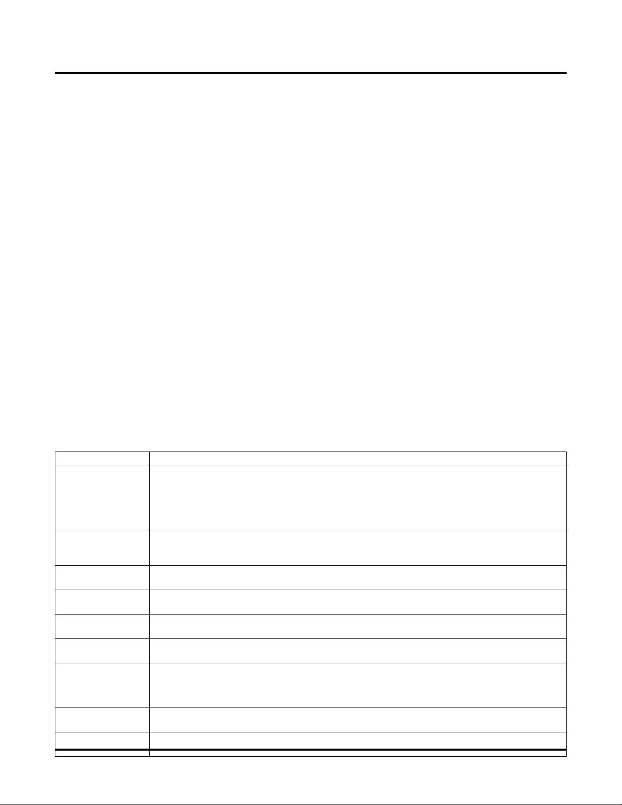
Table 1. LatticeMico8 Synthesis Parameters
Parameter Name Function
FAMILY_NAME
This is a text entry field that is only used during simulation. The value is used to determine the behav-
ioral model to use for instantiated Parameterized Module Instantiation (PMI) elements. Valid entries for
this parameter can be found in the ispLEVER Help. This field is not used during synthesis or place and
route. The target FPGA device can be changed in ispLEVER, and a new FPGA bitstream image gener-
ated without the need to update the FAMILY_NAME entry. ModelSim
®
can override the value in the
HDL using a command line switch when the HDL is compiled.
PROM_FILE
This is a text entry field that determines the opcode data to be loaded into the LatticeMico8 program
memory. This parameter can be explicitly entered in the HDL file, or can be updated as a synthesis
parameter from Synplify
®
, Precision
®
RTL, or ModelSim.
PORT_AW
This defines the number of low order address bits. The value must be less than or equal to 8. The
default value is 8, which permits the LatticeMico8 to address up to 256 external ports.
EXT_AW
This defines the size, in bits, of the external address bus. The parameter must be greater than or equal
to PORT_AW. The default value is 8, which permits the LatticeMico8 to address 256 ports.
PROM_AW
This defines the number of address bits assigned to the LatticeMico8 program memory. The default
value is 9, which permits up to 512 opcodes to be stored.
PROM_AD
This is the number of opcodes the program memory can store and must always be 2^PROM_AW. The
default value is 512 (i.e. 2^9).
REGISTERS_16
This parameter determines how many registers the LatticeMico8 core has. For VHDL the field is a text
entry that can be set to TRUE or FALSE. For Verilog the parameter is an integer field that can be either
0 or 1. When the REGISTERS_16 entry is FALSE/0 the LatticeMico8 will have 32 general purpose reg-
isters. When it is TRUE/1 it will have 16 general purpose registers.
PGM_STACK_AW
This defines the number of address bits assigned to the LatticeMico8 call stack. The default value is 4,
which permits the call stack to hold 16 elements.
PGM_STACK_AD
This defines the depth of the call stack and must always be 2^PGM_STACK_AW. The default value is
16 (i.e. 2^4).


评论1