没有合适的资源?快使用搜索试试~
我知道了~
文库首页
信息化管理
其它
Bumping基础培训资料-Bumping-Basic-Training-Material
Bumping基础培训资料-Bumping-Basic-Training-Material
1.该资源内容由用户上传,如若侵权请联系客服进行举报
2.虚拟产品一经售出概不退款(资源遇到问题,请及时私信上传者)
版权申诉
Bumping
晶圆级封装
5星
· 超过95%的资源
3 下载量
101 浏览量
2022-05-05
21:08:32
上传
评论
3
收藏
2.64MB
PDF
举报
温馨提示
五一特惠:¥22.90
52.90
Bumping基础培训资料-Bumping-Basic-Training-Material
资源推荐
资源详情
资源评论
bumping introduction
浏览:183
5星 · 资源好评率100%
bumping工艺的介绍+国内的bumping工业+回流设备。
Bumping Knowledge
浏览:60
半导体先进封装专业知识,适合于想初步了解这方面的朋友们.
EB_AUTOSAR基础培训EB_AUTOSAR_Basic_Training_Slides_v2018.rar
浏览:178
5星 · 资源好评率100%
EB_AUTOSAR基础培训 3天
matlab代码做游戏-Opencv-Training-Material:Opencv培训资料
浏览:177
matlab代码做游戏学习OpenCV 此存储库包含在我们的博客上共享的有关计算机视觉,深度学习和AI文章的代码。 想要成为AI专家吗? 是一个很好的起点。 博客文章列表 博客文章
chip bumping technology
浏览:174
chip bumping technology
bumping凸块技术与工艺简介.pdf
浏览:158
bumping凸块技术与工艺简介,一些基本的关于芯片制造封装流程方面的东西,基本的芯片相关的入门知识
一种云场景的实时渲染方法
浏览:97
4星 · 用户满意度95%
: 探讨了真实感云场景的模拟技术, 设计了一种云场景...通过引入基于GPU的Bumping纹理算法与Render-to-Texture技术, 极大提高了云场景的渲染速度。实验结果进一步表明该方法能够同时满足真实感与实时性两个方面的要求
半导体的生产工艺流程
浏览:177
微机电制作技术,尤其是最大宗以硅半导体为基础的微细加工技术(silicon- based micromachining),原本就肇源于半导体组件的制程技术,所以必须先介绍清楚这类制程,以免沦于夏虫语冰的窘态。
半导体制冷在测压铜柱高低温校准中的应用.pdf
浏览:156
半导体制冷在测压铜柱高低温校准中的应用.pdf
hmpps-mis-terraform-repo:hmpps-mis-terraform-dev
浏览:133
当分支合并到主节点时也会标记的动作请参见 BumpingManual Bumping: Any commit message that includes #major, #minor, or #patch will trigger the respective version bump. If two or more are present, the ...
pci-swiotlb.rar_The Returned
浏览:138
Keep the generation correct by bumping rptr until it matches the index returned by the rearm - 1.
Dan_Saks_const_T_vs_T_const
浏览:90
bumping into some unknown (by us) rule of the C language. “We are using the Hitachi C com- piler for the Hitachi SH-2 32-bit RISC microcontroller. We thought the fol- lowing code:
Foundation Game Design with Flash
浏览:144
5星 · 资源好评率100%
Foundation Game Design with ...Chapter 7 Bumping into Things Chapter 8 Object-Oriented Game Design Chapter 9 Platform Game: Physics and Data Management Chapter 10 Advanced Object and Character Contro
Unity.in.Action.Multiplatform.Game.Development.in.Csharp
浏览:6
5星 · 资源好评率100%
8.2 Interacting with objects by bumping into them 172 Colliding with physics-enabled obstacles 173 ■ Triggering the door with a pressure plate 174 ■ Collecting items scattered around the level 176 ...
bomping introduction
浏览:163
bumping工艺的介绍+国内的bumping工业+回流设备。 不好意思 这个传错了,不要下载这个了。 我另附上附件。
github-version-generate:用于发布管道中应用程序版本碰撞、生成、读取和格式的 GitHub 操作
浏览:11
GitHub Actions 的版本生成和碰撞 用于在发布管道中读取、碰撞、生成、格式化应用程序版本的 GitHub 操作。 输出三个环境变量: 'env.CURRENT_VERSION' - 没有任何更改的当前提取的应用程序版本 ...
H.265/HEVC标准白皮书(2013年1月)
浏览:37
5星 · 资源好评率100%
C.5.2.3 Picture decoding, marking, additional bumping, and storage 223 C.5.2.4 "Bumping" process 223 Annex D Supplemental enhancement information 225 D.1 General 225 D.2 SEI payload syntax 226 D.2.1
StatusBoard:GitHub供电状态报告
浏览:176
We're bumping to amber _just as a precation_! g 2015-08-26T00:00 No known issues a 2015-08-25T13:04 Ok, slowly coming back online.. r 2015-08-25T13:01 Ah, so _that's_ what a load balancer's for!
英特尔65纳米芯片广泛采用铜柱块凸接合,实现技术领先
浏览:99
半导体芯片与系统反向工程与分析厂商Chipworks日前对英特尔65纳米Presler及Yonah处理器进行分析并宣布发现,微处理器中广泛应用了铜柱块凸接合技术(Copper Pillar Bumping “CPB”),把钢模连接到印制线路板。...
解决win7win8win10装4.8-3.5的.Net framework3.5安装失败问题 附带安装文档
浏览:86
5星 · 资源好评率100%
解决win7win8win10装4.8-3.5的.Net framework3.5安装失败问题 附带安装文档
谷歌浏览器axure扩展程序
浏览:5
3星 · 编辑精心推荐
谷歌浏览器axure扩展程序插件,解压放到谷歌的扩展程序里即可用。
时序图画图工具-TimeGen3.2安装包
浏览:40
免费下载,小巧好用的时序图画图工具TimeGen3.2安装包和安装使用教程,详细的安装和使用教程见博主《数字IC开发工具》栏目的博文。
大唐杯习题合集-历年真题模拟题
浏览:86
总结历年各种大唐杯的题型
Rust的概要介绍与分析
浏览:38
Rust是一种面向对象的编程语言,其设计初衷是为了提供内存安全性,同时保持高性能。Rust拥有强大的类型系统和所有权模型,能够在编译时消除许多常见的内存错误,使得开发者能够编写出既安全又高效的代码。 Rust的资源丰富多样,涵盖了从基础文档到高级库的广泛领域。对于初学者来说,Rust的官方文档提供了详细的语法规则和编程指南,帮助他们快速上手。此外,Rust的社区也非常活跃,有大量的教程和示例代码
百度、高德、腾讯、天地图、谷歌、必应、MapBox等地图金字塔切图工具 MapCutter 3.11.2
浏览:32
百度、高德、腾讯、天地图、谷歌、必应等自定义地图/图片叠加层/瓦片图/金字塔图地图切图高清切片生成工具 MapCutter(旧名MapTiler) ,定位便捷,支持超大地图,支持leaflet、maptalks、openlayers、cesium、及自定义模版输出。 最新版本修正了百度地图的偏差、可调整地图图层的不透明度,、完善webgl输出、支持openlayers、cesium网页输出、支持多
zotero-pdf-translate-1.0.24(2023年7月10日)
浏览:187
zotero的pdf翻译插件
姓名变为拼音.bas
浏览:62
姓名变为拼音.bas WPS或Excel将姓名变为拼音 操作步骤 https://blog.csdn.net/SwTesting/article/details/111690318
CiteSpace5.6.R2,目前最稳定的版本,改时间就可以用
浏览:141
4星 · 用户满意度95%
最稳定版本,没有bug,改时间即可用,分析关键词、作者、机构、关键词聚类、关键词突现、时间线图谱、时区图谱
C#源码 上位机 SECS协议,里面包含各种进制转换,用于半导体行业,程序全源码
浏览:46
C#源码 上位机 SECS协议,里面包含各种进制转换,用于半导体行业,程序全源码
Bumping
T
echnology
Intr
oduction
Prepare By: Mady
W
ang
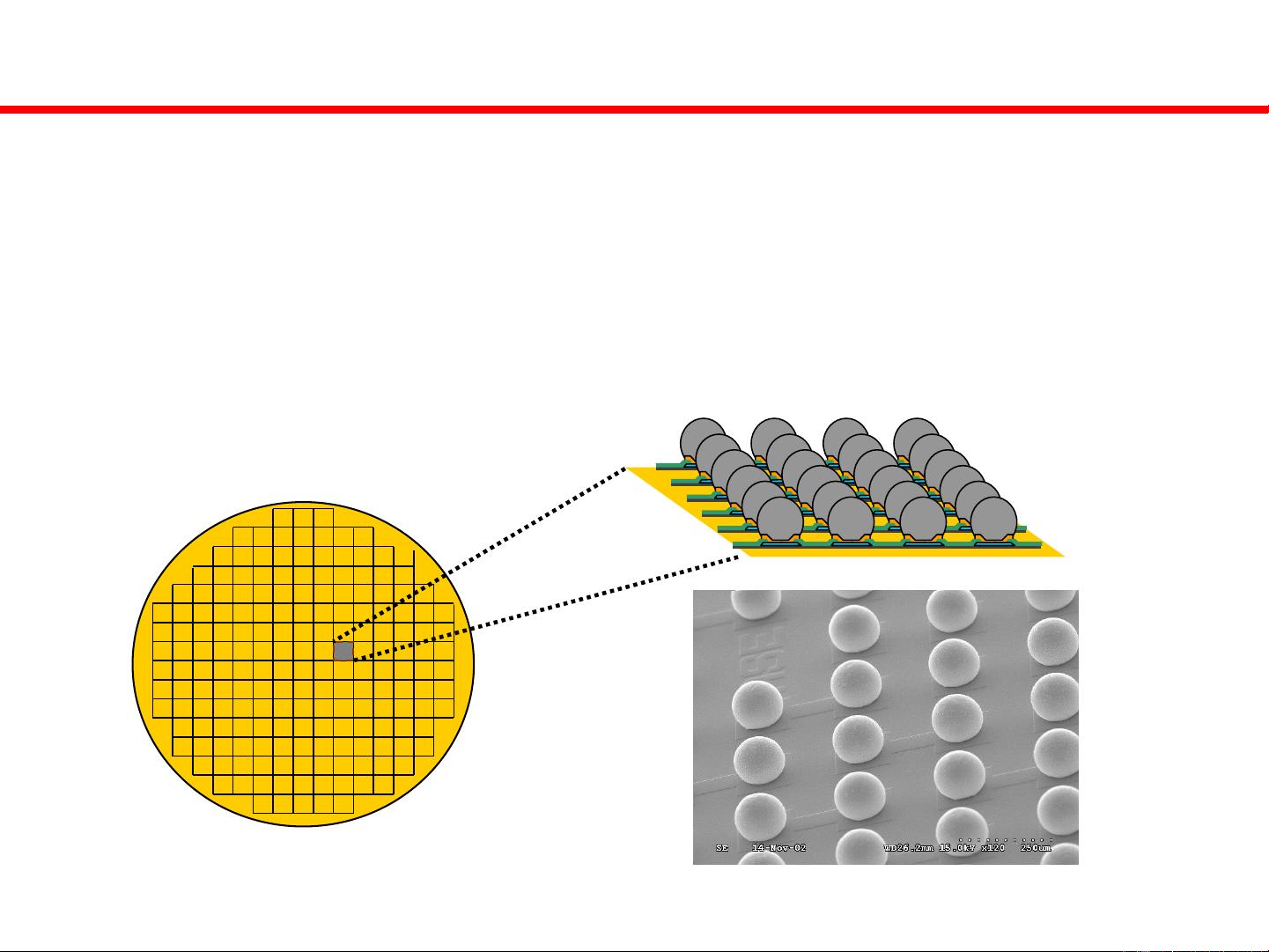
What is Bumping?
•
To generate
bumps on wafer.
•
The essence
to advance
d packaging,
specifica
lly
flip chip packaging.
Benefits of bumping?
•
High density interconnection.
•
High speed data processing
(
short connection
path, lower
connection resistance
and higher driving current
density
)
•
Small package
body size.
•
Real chip size
achievable.
•
Cost competitive.
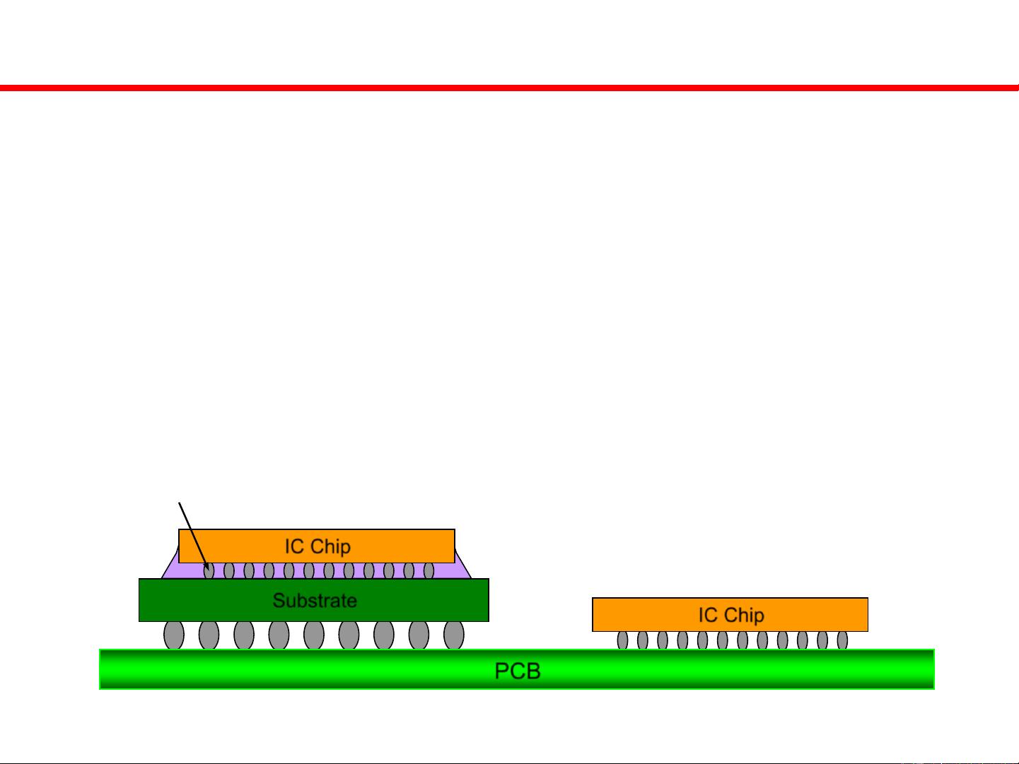
Flip Chip in Package(FCIP)
Flip Chip on Board(FCOB)
IC Chip
Substrate
IC Chip
PCB
Bump
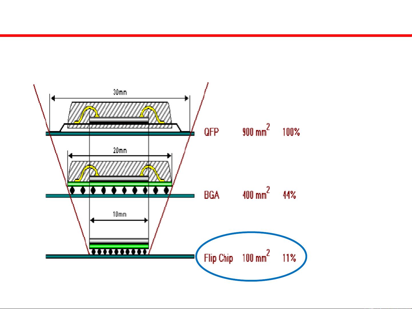
Why Bump Needed
Small outline size
Same chip size but much little
package size with bump process.
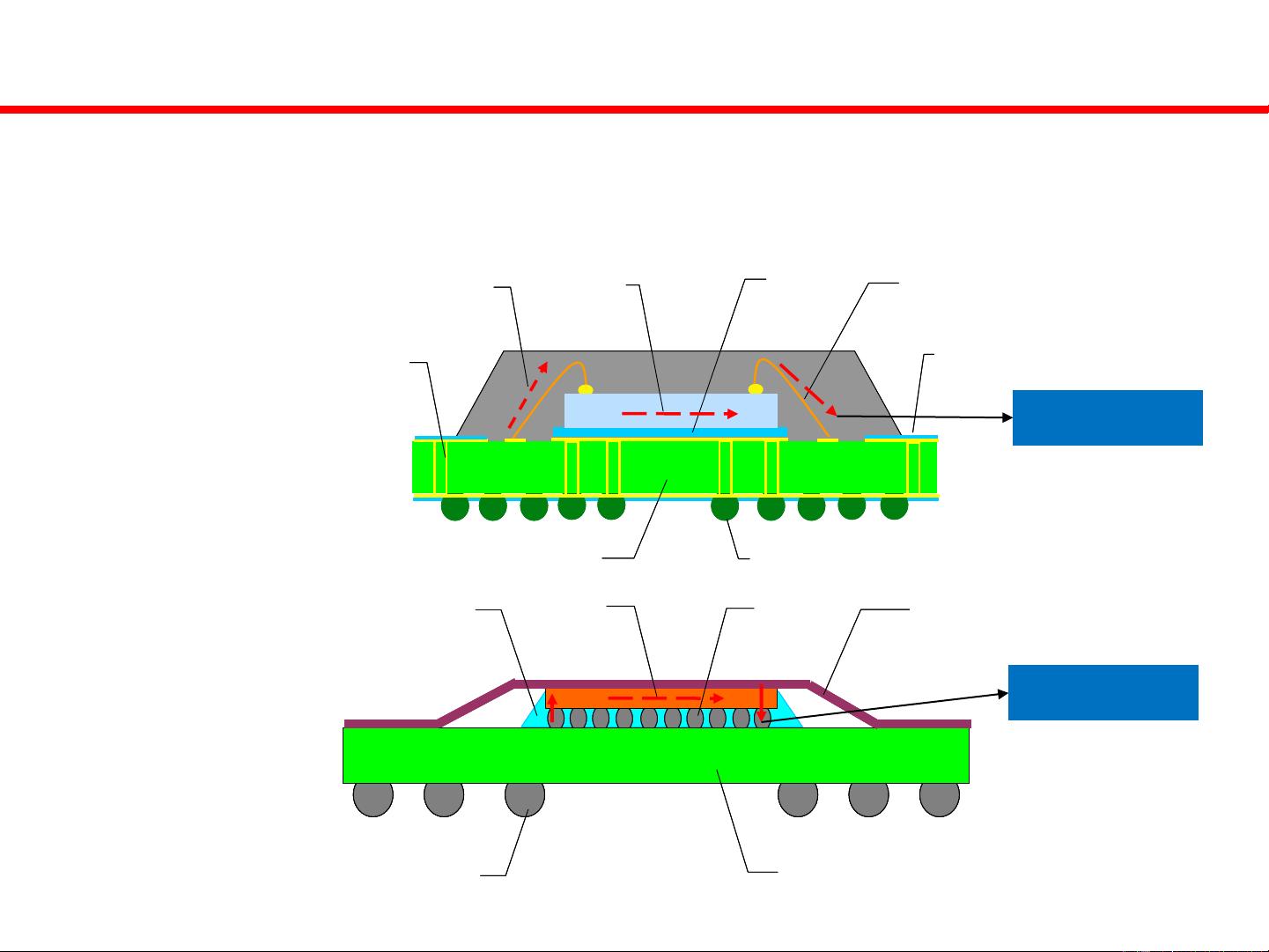
Why Bump Needed
Short signal path
Compared with wire bond, flip chip, which with bump process has shorter signal pa
th.
Chip
Solder b
ump
Underfill
Heat spread
Substrate
Solder b
all
Chip
Solder b
ump
Underfill
Heat spread
Substrate
Solder b
all
signal path
Adhesive
Solder mask
Au wire
Die
Mold compound
Via
Solder ball
Substrate
Adhesive
Solder mask
Au wire
Die
Mold compound
Via
Solder ball
Substrate
signal path
W
ire Bond
Flip Chip
剩余55页未读,
继续阅读
评论
收藏
内容反馈
1.该资源内容由用户上传,如若侵权请联系客服进行举报
2.虚拟产品一经售出概不退款(资源遇到问题,请及时私信上传者)
版权申诉
五一特惠:¥22.90
52.90
资源评论
资源反馈
评论星级较低,若资源使用遇到问题可联系上传者,3个工作日内问题未解决可申请退款~
联系上传者
评论
weixin_41417759
2022-05-23
用户下载后在一定时间内未进行评价,系统默认好评。
树淼
2022-10-31
感谢资源主分享的资源解决了我当下的问题,非常有用的资源。
m0_72977005
2022-08-02
实在是宝藏资源、宝藏分享者!感谢大佬~
pmsecapt
粉丝: 0
资源:
21
私信
上传资源 快速赚钱
我的内容管理
展开
我的资源
快来上传第一个资源
我的收益
登录查看自己的收益
我的积分
登录查看自己的积分
我的C币
登录后查看C币余额
我的收藏
我的下载
下载帮助
前往需求广场,查看用户热搜
最新资源
嵌入式与物联网开发是当今信息技术领域的两大重要分支,它们相互交织,共同推动着智能化时代的进步 嵌入式开发主要关注在嵌入式操作
网络安全,这一看似高深莫测的领域,实则与我们每个人的生活息息相关
毕业设计基于深度学习的视觉问答系统源码+文档说明+答辩PPT.zip
jsp网络在线考试系统(系统).rar
售后服务管理系统【尚学堂·百战程序员】.zip
移动应用开发,作为现代科技领域的一大热门,正以前所未有的速度改变着人们的生活方式 它涵盖了从构思、设计、编程到测试、发布等多个环
数据结构学习-队列/栈
isr.c
dhndfghdghdghdfhfd
爬虫开发的一些·1相关资源
资源上传下载、课程学习等过程中有任何疑问或建议,欢迎提出宝贵意见哦~我们会及时处理!
点击此处反馈
安全验证
文档复制为VIP权益,开通VIP直接复制
信息提交成功


 weixin_414177592022-05-23用户下载后在一定时间内未进行评价,系统默认好评。
 树淼2022-10-31感谢资源主分享的资源解决了我当下的问题,非常有用的资源。 m0_729770052022-08-02实在是宝藏资源、宝藏分享者!感谢大佬~


