


1
1
2
2
3
3
4
4
5
5
A A
B B
C C
D D
Version Control
Version
V0.1
Date
2012/09
Modifications
First release of Schematics
C290PCIe-RDB
Page Description
1 SCHEMATIC PAGE LISTING
2
3
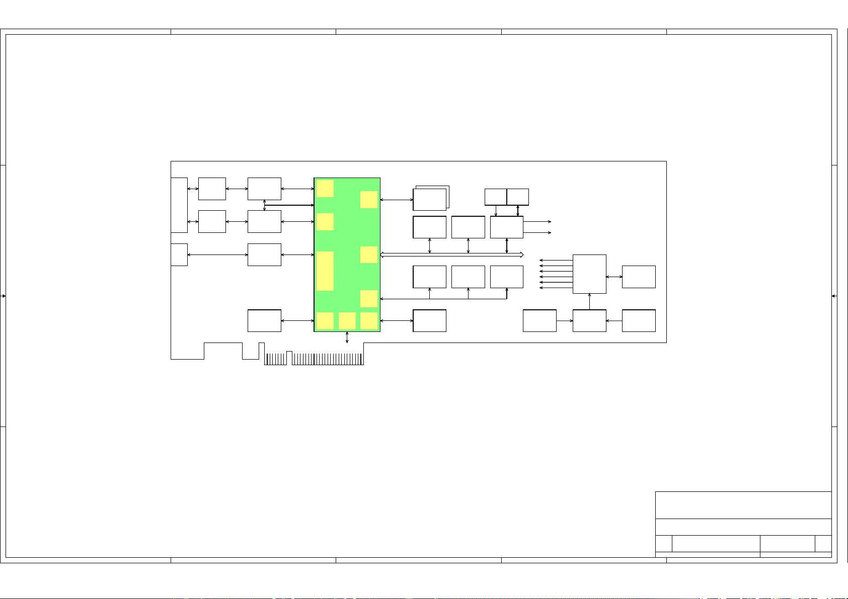
SYSTEM BLOCK DIAGRAM
4
5
6
7
8
9
10
11
12
13
14
15
16
17
18
19
20
21
22
23
24
25
26
27
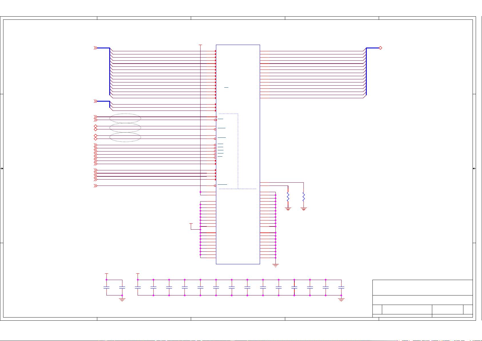
C293 DDR3/DDR3L MEMORY INTERFACE
DDR3/DDR3L MEMORY CHIP 1
DDR3/DDR3L MEMORY CHIP 2
C293 IFC INTERFACE
NOR FLASH and NAND FLASH MEMORY
C293 SERDES and TSEC 1&2 INTERFACE
PCI EXPRESS X4 INTERFACE
10/100/1000 ETHERNET PHY (PORT 1)
10/100/1000 ETHERNET MAGNETICS and RJ45 CONNECTOR (PORT 1)
10/100/1000 ETHERNET PHY (PORT 2)
10/100/1000 ETHERNET MAGNETICS and RJ45 CONNECTOR (PORT 2)
C293 MISC
DUART INTERFACE
C293 POWER-ON STRAPPINGs
C293 POWER SUPPLY
C293 POWER SUPPLY (cont.)
C293 GROUND
CPLD
SYSTEM CLOCK GENERATORs
C293 CORE POWER CONVERTOR
SYSTEM POWER CONVERTORs
SYSTEM POWER INPUT
MECHANICALs
SYSTEM POWER ON SEQUENCING
I2C&SPI DEVICE, RESET and WATCHDOG
V0.2 2012/10
update C293 symbol, change GE phy to VSC8641, add I2C boot EEPROM
V0.3 2012/10
update POR strappings
V0.4 2012/10
1. Change DDR3 to 3 x16 chips. Page 4-6
2. Add FBANK_SEL2 to NOR Flash, change NOR Flash MPN to S29GL512P11TFI0. Page 8
3. Add pull-up resistor to PIN10 of NAND Flash. Page 8
4. Add pull-up resistor to TSEC1_GTX_CLK for cfg_60x in P1010 interposer. Page 8
5. Correct net name errors of "GE2_CMODEx". Page 13
6. Remove UART1 signals and RJ45 connector. Page 15/16
7. Change POR-ON strappings with connect to switchs and CPLD. Page 18/22
8. Connect MGN signal to CPLD and switch to change VCORE voltage. Page 24
9. Change heatsink to S06QZZ0B. Page 28
DDR3/DDR3L MEMORY ECC CHIP
28
V0.5 2012/11
2. Change switch pull-up pull-down resistors to same side.
Page 18/223. Add sw_cfg_rom_loc[0:3] from switch to CPLD.
Page 18
1. Swap DDR3 data bus order for layout. Page 4/5/6
V0.6 2012/11
1. Swap CPLD pins for layout. Page 22
2. Reduce power decoupling caps of C293. Page 20
V0.7 2012/11
1. Generate SOC MVREF use voltage divider. Page 3
2. Delete 4.7pF cap on DDR3 clock pair. Page 3
3. Delete optional pull down resistor for TMP_DETECT_B. Page 15
V0.8 2012/11
1. Add a 0603 cap to 1V0_CB. Page 20
2. Add several caps acrossing plane splits. Page 28
V0.9 2012/12
1. Add a 1000pF cap between ZL_VSEN_P and ZL_VSEN_N. Page 24
2. Change U34 to SOT23-5 footprint and connect NC pin to GND. Page 25
V1.0 2013/02
update BOM
V1.1 2013/02
1. Change NAND Flash R/B to CPLD, then CPLD to C293 R/B0 and R/B1. Page 7/8/22
2. Add a 0.01uF cap to PEX_RST_N. Page 10
3. Change panel LED to single color. Page 22
V2.0 2013/08
Add 6pin ATX 6pin power connector, remove PTC and common mode chock Page 25
V2.1 2013/10
Add notes for serdes power and nand flash
stuff R248, R275, R299,
V3.0 2013/12
Add 1.0V LDO for SVDD
Title
Size Document Number Rev
Date: Sheet
of
Design Engineer
<Doc> A
<Title>
B
128Tuesday, January 07, 2014
MICETEK
Title
Size Document Number Rev
Date: Sheet
of
Design Engineer
<Doc> A
<Title>
B
128Tuesday, January 07, 2014
MICETEK
Title
Size Document Number Rev
Date: Sheet
of
Design Engineer
<Doc> A
<Title>
B
128Tuesday, January 07, 2014
MICETEK