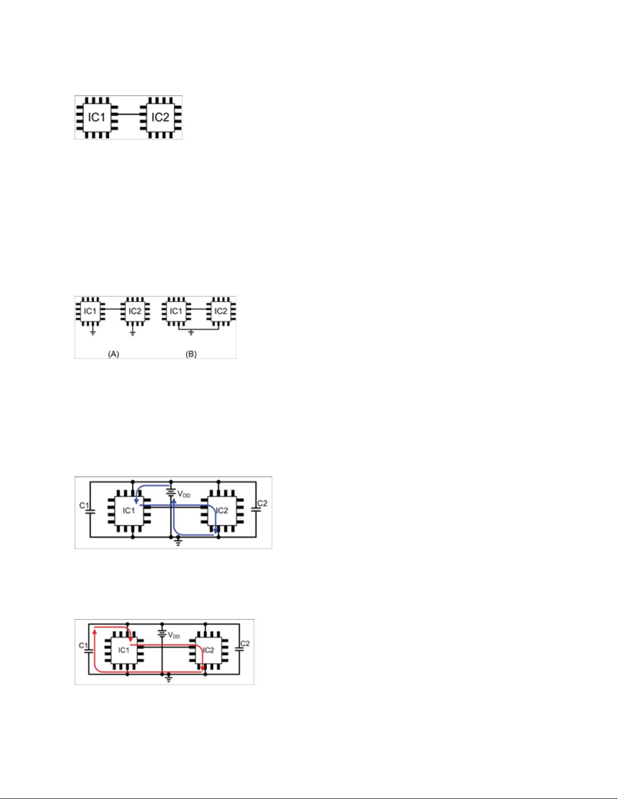
transient currents are just as fast as with a much higher frequency signal. They simply do not occur as often.
Of course, we are dealing with a good design here, so the bypass capacitors and the IC power and ground
pins are very close. Proper bypassing like this makes a designer's job much easier. We can usually just think
of the bypass capacitor and the IC as one entity when considering the flow of signal currents across a PCB.
Notice, finally, that the power current for high-speed AC signals travels a very short distance from a bypass
capacitor to the IC that it is bypassing. The paths through the ICs themselves, of course, are short. The vast
majority of the distance of the current loop is in the interconnect from the output of one chip to the input of the
other and the ground return path. Review Figure 4 and Figure 5 and consider what happens if the ICs are
separated by a greater distance. The bypass capacitors stay close to their respective IC, and all the distance
is added to the interconnect and the ground return. For higher-speed signal currents, this is where we will see
problems…if they occur.
Digital and Analog Supplies and Grounds
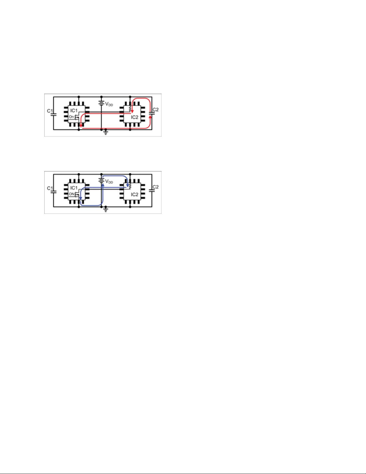
In the circuit diagrams above we have not identified the ICs and signals as digital or analog. IC1 could be an
op amp with the low-side FET as the lower part of an output stage; the pin on IC2 could be the input to an
analog-to-digital converter (ADC). IC1 could just as easily be a microcontroller with a push-pull output for a
standard I/O pin; the IC2 input could be a control pin on a digital-to-analog converter (DAC).
We mention ADCs and DACs as these are typically the components that cause concerns with grounding for
both the analog and digital signals.
Analog circuits tend to work with signals that vary in a smoother, continuous fashion and for which small
changes in voltage or current are meaningful. Digital circuits tend to transition abruptly from one state to
another, generating pulses of currents; they tend to have a wide window of voltage which maps to a single
state. It is these relatively large, sharp pulses of digital current during transitions that can overwhelm the
precise analog signals if the two are not adequately separated from each other.
The Path of Least Impedance
It is such a well-understood principal that current flows in the path of least resistance that the concept has
made its way into everyday language. Unfortunately, this is only true for DC currents. A more complete and
accurate way of stating the principle is that the current flows in the path of least impedance.
For DC, only the resistive part of impedance matters. In the case of a solid ground plane, the proverbial
straight line is the path of least resistance. In fact current will flow in more indirect paths as well. The amount
of current through any particular path will be inversely proportional to the distance because the ground-plane
resistance per unit length is very uniform. Therefore, the most current will flow in the straight-line path of least
resistance, and progressively less current will flow through paths that deviate more and more from that
straight-line path. For simplicity we will indicate DC currents as flowing in the straight line path, with the
understanding that there is a fairly wide spread of currents with the largest current moving along that straight
line.
For the signals that matter most to us here, the AC signals of some speed, we have to consider the reactive
portion of impedance as well.
For a PCB with a ground-plane layer adjacent to the signal layer, we have a well-defined impedance that is
determined by the geometry of the trace, the thickness of the board layer that separates the trace from the
ground plane, the board material, and the frequency of the signal. All the mathematical details for these


 我的内容管理
展开
 我的资源
快来上传第一个资源
 我的收益 登录查看自己的收益
 我的积分
登录查看自己的积分
 我的C币
登录后查看C币余额
 我的收藏
我的收藏  我的下载
我的下载  下载帮助
下载帮助 
 前往需求广场,查看用户热搜

 信息提交成功