没有合适的资源?快使用搜索试试~ 我知道了~
FDC2214电容传感器芯片数据手册
需积分: 5 0 下载量 85 浏览量
2024-11-15
09:56:33
上传
评论
收藏 1.87MB PDF 举报
温馨提示
内容概要:本文档为FDC2214数据手册,详细介绍了FDC2214芯片的技术规格与参数。主要涵盖传感器接口电路(如I2C Resonant Circuit Driver)的设计及特性,以及在近距检测与液位测量等领域中的应用方法。FDC2214是一种高分辨率、高精度的12位电磁兼容抗扰型电容数字转换器。它支持多通道配置,并能在高噪声环境中稳定运行。此外,文档还提供了关于如何设定寄存器值、调整参数以及进行误差处理的方法。 适合人群:嵌入式系统开发者、硬件工程师、从事传感技术研发的相关技术人员。 使用场景及目标:用于开发高性能传感设备时选择合适的芯片型号并了解其具体性能指标。通过掌握设置方法优化系统架构与程序设计流程。 其他说明:文中涉及的技术细节对于理解和使用本系列产品的关键功能至关重要,同时也可以作为同类产品对比时的重要参考资料。文档还提供了一些实际案例帮助使用者更好地理解产品特性和应用场景。
资源推荐
资源详情
资源评论

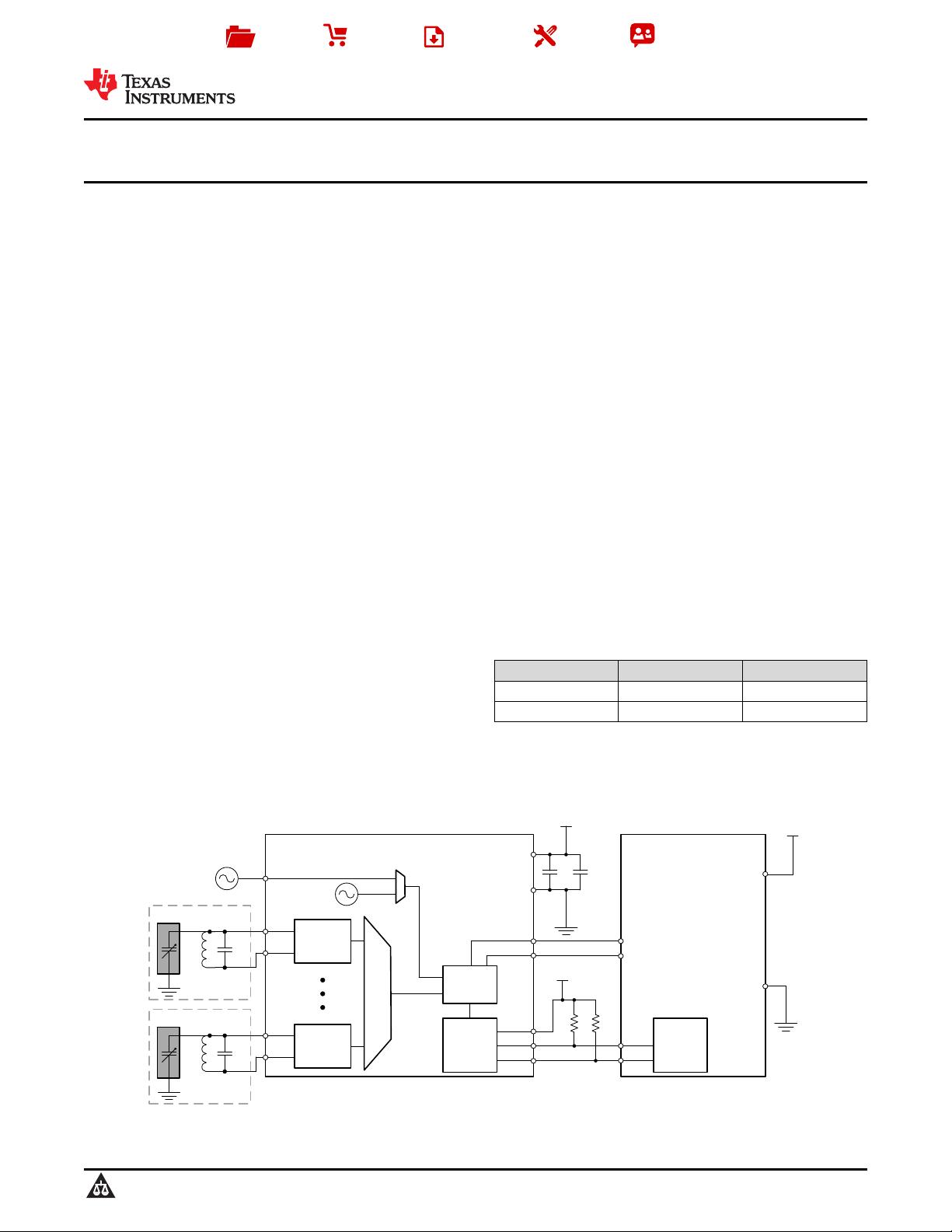
IN0A
IN0B
IN3A
IN3B
FDC2114 / FDC2214
VDD
GND
SCL
SDA
Int. Osc.
ADDR
INTB
SD
GND
MCU
VDD
3.3 V
3.3 V
GPIO
GPIO
0.1 F 1 F
Core
I
2
C
I
2
C
peripheral
3.3 V
L
Cap
Sensor 0
CLKIN
40 MHz
C
L
Cap
Sensor 3
C
Resonant
circuit driver
Resonant
circuit driver
Product
Folder
Sample &
Buy
Technical
Documents
Tools &
Software
Support &
Community
FDC2212
,
FDC2214
,
FDC2112
,
FDC2114
SNOSCZ5A –JUNE 2015–REVISED JUNE 2015
FDC2x1x EMI-Resistant 28-Bit,12-Bit Capacitance-to-Digital Converter for Proximity and
Level Sensing Applications
1 Features 3 Description
Capacitive sensing is a low-power, low-cost, high-
1
• EMI-Resistant Architecture
resolution contactless sensing technique that can be
• Maximum Output Rates (one active channel):
applied to a variety of applications ranging from
– 13.3 ksps (FDC2112, FDC2114)
proximity detection and gesture recognition to remote
liquid level sensing. The sensor in a capacitive
– 4.08 ksps (FDC2212, FDC2214)
sensing system is any metal or conductor, allowing
• Maximum Input Capacitance: 250 nF (at 10 kHz
for low cost and highly flexible system design.
with 1 mH inductor)
The main challenge limiting sensitivity in capacitive
• Sensor Excitation Frequency: 10 kHz to 10 MHz
sensing applications is noise susceptibility of the
• Number of channels: 2, 4
sensors. With the FDC2x1x innovative EMI resistant
• Resolution: up to 28 bits
architecture, performance can be maintained even in
presence of high-noise environments.
• System Noise Floor: 0.3 fF at 100 sps
• Supply Voltage: 2.7 V to 3.6 V
The FDC2x1x is a multi-channel family of noise- and
EMI-resistant, high-resolution, high-speed
• Power Consumption: Active: 2.1 mA
capacitance-to-digital converters for implementing
• Low-Power Sleep Mode: 35 uA
capacitive sensing solutions. The devices employ an
• Shutdown: 200 nA
innovative narrow-band based architecture to offer
high rejection of noise and interferers while providing
• Interface: I
2
C
high resolution at high speed. The devices support a
• Temperature range: -40°C to +125°C
wide excitation frequency range, offering flexibility in
system design. A wide frequency range is especially
2 Applications
useful for reliable sensing of conductive liquids such
as detergent, soap, and ink.
• Proximity Sensor
• Gesture Recognition
Device Information
(1)
• Level Sensor for Liquids, including Conductive
PART NUMBER PACKAGE BODY SIZE (NOM)
ones such as Detergent, Soap, and Ink
FDC2112, FDC2212 WSON (DNT 12) 4.00 mm x 4.00 mm
• Collision Avoidance
FDC2114, FDC2214 WQFN (RGH 16) 4.00 mm x 4.00 mm
• Rain, Fog, Ice, Snow Sensor
(1) For all available packages, see the orderable addendum at
• Automotive Door and Kick Sensors
the end of the datasheet.
• Material Size Detection
Simplified Schematic
1
An IMPORTANT NOTICE at the end of this data sheet addresses availability, warranty, changes, use in safety-critical applications,
intellectual property matters and other important disclaimers. PRODUCTION DATA.

FDC2212
,
FDC2214
,
FDC2112
,
FDC2114
SNOSCZ5A –JUNE 2015–REVISED JUNE 2015
www.ti.com
Table of Contents
9.4 Device Functional Modes........................................ 21
1 Features.................................................................. 1
9.5 Programming........................................................... 21
2 Applications ........................................................... 1
9.6 Register Maps......................................................... 22
3 Description ............................................................. 1
10 Application and Implementation........................ 39
4 Revision History..................................................... 2
10.1 Application Information.......................................... 39
5 Description, continued.......................................... 3
10.2 Typical Application ............................................... 40
6 Device Comparison Table..................................... 3
10.3 Do's and Don'ts..................................................... 46
7 Pin Configuration and Functions......................... 4
11 Power Supply Recommendations ..................... 46
8 Specifications......................................................... 5
12 Layout................................................................... 46
8.1 Absolute Maximum Ratings ...................................... 5
12.1 Layout Guidelines ................................................. 46
8.2 ESD Ratings ............................................................ 5
12.2 Layout Example .................................................... 46
8.3 Recommended Operating Conditions....................... 5
13 Device and Documentation Support ................. 51
8.4 Thermal Information ................................................. 5
13.1 Device Support...................................................... 51
8.5 Electrical Characteristics........................................... 6
13.2 Related Links ........................................................ 51
8.6 Timing Requirements................................................ 7
13.3 Community Resources.......................................... 51
8.7 Switching Characteristics - I2C ................................. 8
13.4 Trademarks........................................................... 51
8.8 Typical Characteristics.............................................. 9
13.5 Electrostatic Discharge Caution............................ 51
9 Detailed Description............................................ 11
13.6 Glossary................................................................ 51
9.1 Overview ................................................................. 11
14 Mechanical, Packaging, and Orderable
9.2 Functional Block Diagrams ..................................... 11
Information ........................................................... 51
9.3 Feature Description................................................. 12
4 Revision History
Changes from Original (June 2015) to Revision A Page
• Added full datasheet. ............................................................................................................................................................. 1
2 Submit Documentation Feedback Copyright © 2015, Texas Instruments Incorporated
Product Folder Links: FDC2212 FDC2214 FDC2112 FDC2114

FDC2212
,
FDC2214
,
FDC2112
,
FDC2114
www.ti.com
SNOSCZ5A –JUNE 2015–REVISED JUNE 2015
5 Description, continued
The FDC221x is optimized for high resolution, up to 28 bits, while the FDC211x offers fast sample rate, up to
13.3ksps, for easy implementation of applications that use fast moving targets. The very large maximum input
capacitance of 250 nF allows for the use of remote sensors, as well as for tracking environmental changes over
time, temperature and humidity.
The FDC2x1x family targets proximity sensing and liquid level sensing applications for any type of liquids. For
non-conductive liquid level sensing applications in the presence of interferences such as human hands, the
FDC1004 is recommended, which has integrated active shield drivers.
6 Device Comparison Table
PART NUMBER RESOLUTION CHANNELS PACKAGE
FDC2112 12 bit 2 WSON-12
FDC2114 12 bit 4 WQFN-16
FDC2212 28 bit 2 WSON-12
FDC2214 28 bit 4 WQFN-16
Copyright © 2015, Texas Instruments Incorporated Submit Documentation Feedback 3
Product Folder Links: FDC2212 FDC2214 FDC2112 FDC2114

1
2
3
4
12
11
10
9
5
6
7
8
16
15
14
13
DAP
SCL
SDA
CLKIN
ADDR IN0A
IN0B
IN1A
IN1B
INTB
SD
VDD
GND
IN3B
IN2B
IN3A
IN2A
DAP
1SCL
3CLKIN
4ADDR
INTB 5
VDD7
GND8
IN0A9
IN0B
10
IN1A11
SD 6
IN1B12
2SDA
FDC2212
,
FDC2214
,
FDC2112
,
FDC2114
SNOSCZ5A –JUNE 2015–REVISED JUNE 2015
www.ti.com
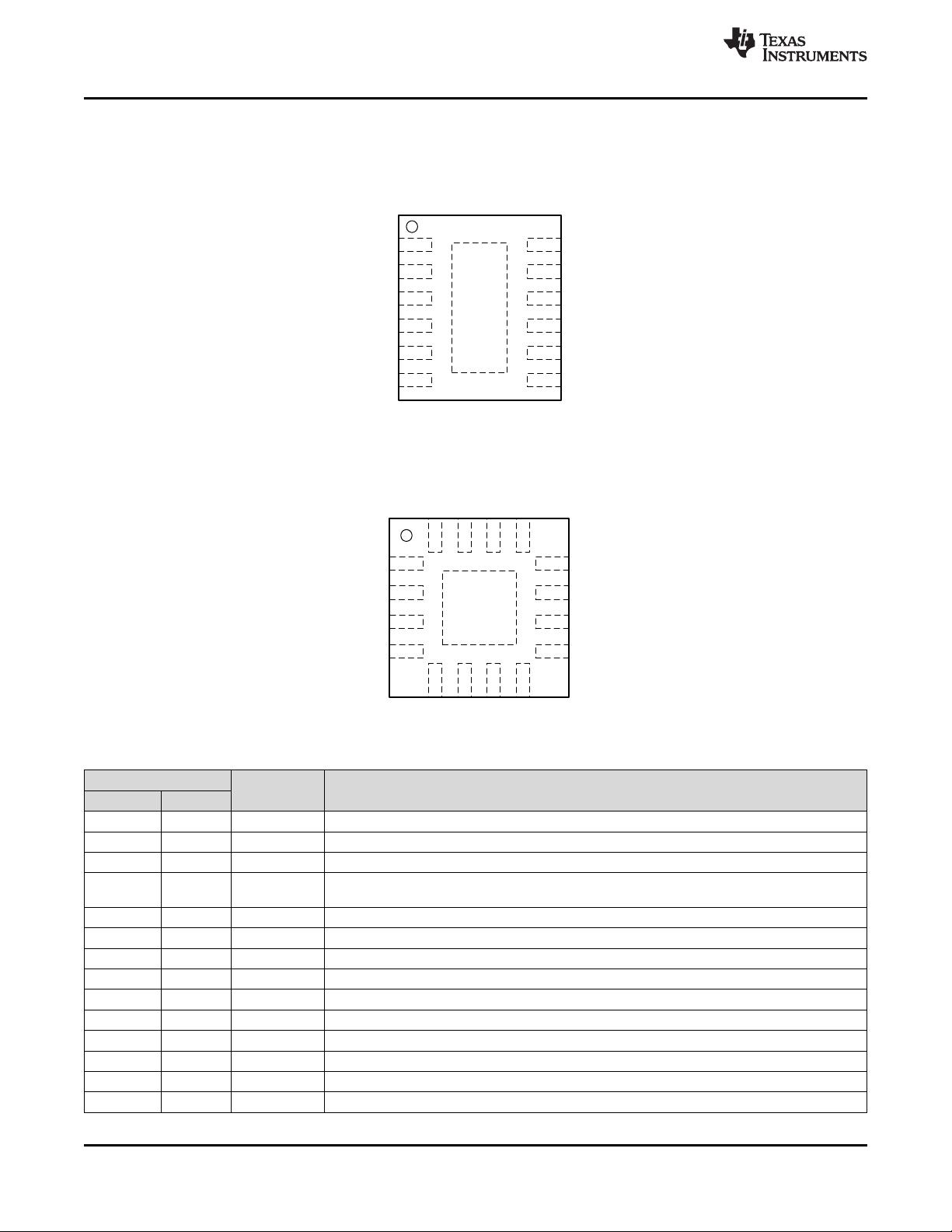
7 Pin Configuration and Functions
FDC2112/FDC2212 WSON
DNT-12
Top View
FDC2114/FDC2214 WQFN
RGH-16
Top View
Pin Functions
PIN
TYPE
(1)
DESCRIPTION
NAME NO.
SCL 1 I I2C Clock input
SDA 2 I/O I2C Data input/output
CLKIN 3 I Master Clock input. Tie this pin to GND if internal oscillator is selected
I2C Address selection pin: when ADDR=L, I2C address = 0x2A, when ADDR=H, I2C address =
ADDR 4 I
0x2B.
INTB 5 O Configurable Interrupt output pin
SD 6 I Shutdown input
VDD 7 P Power Supply
GND 8 G Ground
IN0A 9 A Capacitive sensor input 0
IN0B 10 A Capacitive sensor input 0
IN1A 11 A Capacitive sensor input 1
IN1B 12 A Capacitive sensor input 1
IN2A 13 A Capacitive sensor input 2 (FDC2114 / FDC2214 only)
IN2B 14 A Capacitive sensor input 2 (FDC2114 / FDC2214 only)
(1) I = Input, O = Output, P=Power, G=Ground, A=Analog
4 Submit Documentation Feedback Copyright © 2015, Texas Instruments Incorporated
Product Folder Links: FDC2212 FDC2214 FDC2112 FDC2114

FDC2212
,
FDC2214
,
FDC2112
,
FDC2114
www.ti.com
SNOSCZ5A –JUNE 2015–REVISED JUNE 2015
Pin Functions (continued)
PIN
TYPE
(1)
DESCRIPTION
NAME NO.
IN3A 15 A Capacitive sensor input 3 (FDC2114 / FDC2214 only)
IN3B 16 A Capacitive sensor input 3 (FDC2114 / FDC2214 only)
DAP
(2)
DAP N/A Connect to Ground
(2) There is an internal electrical connection between the exposed Die Attach Pad (DAP) and the GND pin of the device. Although the DAP
can be left floating, for best performance the DAP should be connected to the same potential as the device's GND pin. Do not use the
DAP as the primary ground for the device. The device GND pin must always be connected to ground.
8 Specifications
8.1 Absolute Maximum Ratings
MIN MAX UNIT
VDD Supply voltage range 5 V
Vi Voltage on any pin –0.3 VDD + 0.3 V
IA Input current on any INx pin –8 8 mA
ID Input current on any digital pin –5 5 mA
T
J
Junction temperature –55 150 °C
T
stg
Storage temperature –65 150 °C
(1) Stresses beyond those listed under Absolute Maximum Ratings may cause permanent damage to the device. These are stress ratings
only, which do not imply functional operation of the device at these or any other conditions beyond those indicated under Recommended
Operating Conditions. Exposure to absolute-maximum-rated conditions for extended periods may affect device reliability.
8.2 ESD Ratings
VALUE UNIT
FDC2112 / FDC2212 in 12-pin WSON package
Human-body model (HBM), per ANSI/ESDA/JEDEC JS-001
(1)
±2000
V
(ESD)
Electrostatic discharge V
Charged-device model (CDM), per JEDEC specification JESD22- ±750
C101
(2)
FDC2114 / FDC2214 in 16-pin WQFN package
Human-body model (HBM), per ANSI/ESDA/JEDEC JS-001
(1)
±2000
V
(ESD)
Electrostatic discharge V
Charged-device model (CDM), per JEDEC specification JESD22- ±750
C101
(2)
(1) JEDEC document JEP155 states that 500-V HBM allows safe manufacturing with a standard ESD control process.
(2) JEDEC document JEP157 states that 250-V CDM allows safe manufacturing with a standard ESD control process.
8.3 Recommended Operating Conditions
Unless otherwise specified, all limits ensured for T
A
= 25°C, VDD = 3.3 V
MIN NOM MAX UNIT
VDD Supply voltage 2.7 3.6 V
T
A
Operating temperature –40 125 °C
8.4 Thermal Information
FDC2112 / FDC2214 /
FDC2212 FDC2214
THERMAL METRIC
(1)
UNIT
DNT (WSON) RGH (WQFN)
12 PINS 16 PINS
R
θJA
Junction-to-ambient thermal resistance 50 38 °C/W
(1) For more information about traditional and new thermal metrics, see the Semiconductor and IC Package Thermal Metrics application
report, SPRA953.
Copyright © 2015, Texas Instruments Incorporated Submit Documentation Feedback 5
Product Folder Links: FDC2212 FDC2214 FDC2112 FDC2114
剩余60页未读,继续阅读
资源评论

晨之清风
- 粉丝: 5789
- 资源: 67
上传资源 快速赚钱
 我的内容管理
展开
 我的资源
快来上传第一个资源
 我的收益 登录查看自己的收益
 我的积分
登录查看自己的积分
 我的C币
登录后查看C币余额
 我的收藏
我的收藏  我的下载
我的下载  下载帮助
下载帮助

 前往需求广场,查看用户热搜
最新资源
- opencv-4.10.0-vs2022-x86 音视频研发
- 2015-2016中国手机应用商店年度报告.pdf
- 2015-2016中国信息时代新消费方式专题报告.pdf
- 2015Q3Q4中国TMT报告.pdf
- 2015Q4中国移动社交通信季度报告.pdf
- springboot学生作业管理系统.zip
- 基于Python+Flask开发的Android测试工具
- 2015本地出行类移动应用行业分析报告.pdf
- 2015埃维诺技术展望.pdf
- 解决ole DB 保存nvarchar字符乱码问题
- 2015国产电影发行市场白皮书.pdf
- 2015大地影院媒体生态圈价值报告(完整版).pdf
- 河北省雄安新区(马蹄湾村)航空高光谱遥感应用数据集下载
- 2015美国新媒体研究报告(皮尤研究中心).pdf
- 2015年1-4月中国移动互联网行业发展分析报告.pdf
- 2015年1月至11月微博移动端用户研究报告.pdf
资源上传下载、课程学习等过程中有任何疑问或建议,欢迎提出宝贵意见哦~我们会及时处理!
点击此处反馈


安全验证
文档复制为VIP权益,开通VIP直接复制
 信息提交成功