没有合适的资源?快使用搜索试试~ 我知道了~
HX8363-A_AN_v02_100915--17.pdf
需积分: 9 11 下载量 7 浏览量
2020-05-16
17:18:29
上传
评论 1
收藏 898KB PDF 举报
温馨提示
试读
28页
HX8363A 应用手册, 不是规格书。 分辨率800*480的一个屏幕 应用手册里附带了初始化程序。
资源推荐
资源详情
资源评论
HX8363-A (N)
480RGB x 864 dot, 16.7M color,
TFT Mobile Single Chip Driver
Preliminary version 02 September, 2010
( DOC No. HX8363
-
A
-
AN)
For 幸福里 Only
- P.1-
H
i
m
a
x Confidential
This information contained herein is the exclusive property of Himax and shall not be distributed, reproduced, or disclosed
in whole or in part without prior written permission of Himax. September, 2010
1. Reference FPC Circuit and Initial Code ............................................................................................4
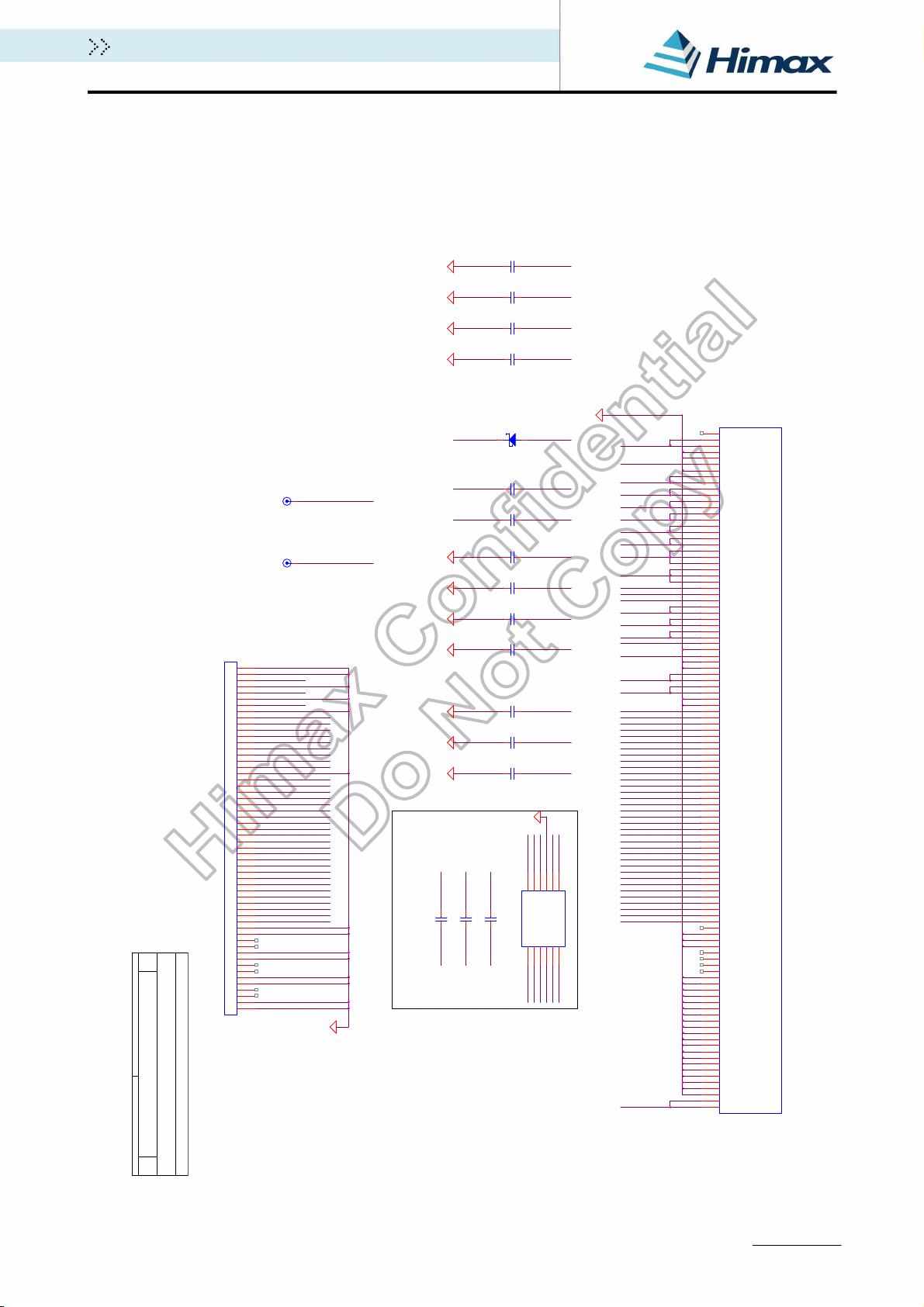
1.1 Reference for CMI’s F03508-01V panel.......................................................................................4
1.1.1 SPI+RGB I/F with HX5186-A reference FPC circuit ................................................................4
1.1.2 DSI I/F with HX5186-A reference FPC circuit ..........................................................................5
1.1.3 The reference setting of normal display for HX5186-A............................................................6
1.1.4 SPI+RGB I/F with PFM mode reference FPC circuit ...............................................................8
1.1.5 DSI I/F with PFM mode reference FPC circuit.........................................................................9
1.1.6 The reference setting of normal display for PFM mode.........................................................10
1.2 Reference for CPT’s 038LA31 panel .........................................................................................12
1.2.1 SPI+RGB I/F with HX5186-A reference FPC circuit ..............................................................12
1.2.2 DSI I/F with HX5186-A reference FPC circuit ........................................................................13
1.2.3 The reference setting of normal display for HX5186-A..........................................................14
2. Code For Reference..........................................................................................................................16
2.1 Sleep in(10h) ..............................................................................................................................16
2.2 Sleep out (11h) ...........................................................................................................................16
2.3 Display off (28h) .........................................................................................................................16
2.4 Display on (29h) .........................................................................................................................16
2.5 CABC on.....................................................................................................................................17
2.5.1 UI mode..................................................................................................................................17
2.5.2 Still mode................................................................................................................................17
2.5.3 Moving mode..........................................................................................................................17
2.6 CABC off.....................................................................................................................................18
3. OTP Programing................................................................................................................................19
3.1 OTP Table...................................................................................................................................19
3.2 OTP programming flow ..............................................................................................................23
3.3 Programming sequence .............................................................................................................24
3.4 OTP Programming Circuitry .......................................................................................................26
4. Revision History................................................................................................................................27
HX8363-A (N)
480RGB x 864 dot, 16.7M color, TFT
Mobi
le Single Chip Driver
List of Contents
Sep, 2010
For 幸福里 Only
- P.2-
H
i
m
a
x Confidential
This information contained herein is the exclusive property of Himax and shall not be distributed, reproduced, or disclosed
in whole or in part without prior written permission of Himax.
September, 2010
Figure 1.1 HX8363-A SPI+RGB I/F with HX5186-A Reference FPC Circuit for CMI panel.........4
Figure 1.2 HX8363-A DSI I/F with HX5186-A Reference FPC Circuit for CMI panel...................5
Figure 1.3 HX8363-A SPI+RGB I/F with PFM mode Reference FPC Circuit for CMI panel........8
Figure 1.4 HX8363-A DSI I/F with PFM mode Reference FPC Circuit for CMI panel .................9
Figure 1.5 HX8363-A SPI+RGB I/F with HX5186-A Reference FPC Circuit for CPT panel ......12
Figure 1.6 HX8363-A DSI I/F with HX5186-A Reference FPC Circuit for CPT panel................13
Figure 3.1 OTP Programming Sequence...................................................................................23
Fig
ure 3.2 OTP Programming Circuitry......................................................................................26
HX8363-A (N)
480RGB x 864 dot, 16.7M color, TFT
Mobi
le Single Chip Driver
List of Contents
Sep, 2010
200
9
For 幸福里 Only
- P.3-
H
i
m
a
x Confidential
This information contained herein is the exclusive property of Himax and shall not be distributed, reproduced, or disclosed
in whole or in part without prior written permission of Himax. September, 2010
Table 3.1 OTP Programming sequence .....................................................................................25
HX8363-A (N)
480RGB x 864 dot, 16.7M color, TFT
Mobile Single Chip Driver
List of Contents
Sep, 2010
200
9
For 幸福里 Only
- P.4-
H
i
m
a
x Confidential
This information contained herein is the exclusive property of Himax and shall not be distributed, reproduced, or disclosed
in whole or in part without prior written permission of Himax. September, 2010
HX8363-A (N)
480RGBx864dots, TFT Mobile Single Chip Driver
APPLICATION NOTE V02
DATA
SHEET
P
reliminary V0
1
1. Reference FPC Circuit and Initial Code
1.1 Reference for CMI’s F03508-01V panel
1.1.1 SPI+RGB I/F with HX5186-A reference FPC circuit
F
i
g
u
re 1.1 HX8363-A SPI+RGB I/F with HX5186-A Reference FPC Circuit for CMI panel
Title
Size Document Number Rev
Date: Sheet
of
<Doc> 1.0
HX8363-A
Custom
1 1Monday, December 07, 2009
DOTCLK
HSYNC
VSYNC
VSN
VCC
DB18
DB2
VSN VGL
D2
RB521S-30
12
CABC_PWM_OUT
DB10
VSPR
DB19
VCOM
DB3
VCC
VSNR
PVSS1
PVSS
CABC_PWM_OUT1
CABC_PWM_OUT
DB11
NRESET
VDDDN
NOTES
3
:
::
:
Set PCCS1,PCCS0="10"
HX5186-A mode.
C3
1u/25V
C9
1u/6V
C10
1u/6V
C4
1u/25V
DGND
VCC
C12
1u/6V
DGND
VSN
C18
2.2u/10V
DGND
VSP
C19
2.2u/10V
VDDDN
VSNR
DGNDDGNDDGND
VSPR
C7
1u/10V
C8
1u/10V
C5
1u/16V
C6
1u/16V
VDDD
DGND
C22AP
C2
1u/5V
C1
2.2u/6V
DGNDDGND
C21AP
DGNDDGND
VCOM
VGL
VGH
C21AN
C22AN
VREF
DB20
DB4
CABC_PWM_OUT
DB12
CABC_PWM_OUT
DB21
DB5
VREF
NOTES
1
:
::
:
Set BS1,BS0="00"
3 wire serial +
RGB interface mode.
VCSW1
PVSS
DGND
DB13
VDDD
VCSW2
NOTES
2
:
::
:
Set RSO2,RSO1,RSO0,="010"
on panel side.
Panel resolution is
480RGBx800.
C22AN
DB22
SDO
DB6
IOVCC
C13 1u/10V
C14 1u/10V
VSN
VSP
VCC
VCSW2
VCSW1
C15 1u/10V
C2P
C3NC3P
C1NC1P
C2N
C1P
C2N
C2P
C3N
C3P
C1N
U2
HX5186-A
VSP
1
VSN
2
GND
3
CTRL_A
4
CTRL_B
5
VIN
6
C1N
7
C1P
8
C2N
9
C2P
10
C3N
11
C3P
12
DB19
DB10
DB2
DB18
DB12
DB4
DB20
DB11
DB3
DB6
DB22
DB13
DB5
DB21
DB16
DB8
DB15
DB7
DB23
DB14
C22AP
DB1
DB17
DB9
DB0
DB14
VCC
SDI
J1
CONN FLEX 56
1
2
3
4
5
6
7
8
9
10
11
12
13
14
15
16
17
18
19
20
21
22
23
24
25
26
27
28
29
30
31
32
33
34
35
36
37
38
39
40
41
42
43
44
45
46
47
48
49
50
51
52
53
54
55
56
DB23
C21AN
PVSS
DB7
C21AP
DB15
IOVCC
SDI
SDO
ENABLE
DOTCLK
HSYNC
VSYNC
NRESET
SCL
NCS
VCC
VGH
NCS
DGND
DB8
U1
HX8363-A
VCOMR
110
VCOM
109
VCOM
108
VSSA
107
VSSA
106
VREF
105
VSSAC
104
VGH
103
VGH
102
VGL
101
VGL
100
C22AN
99
C22AN
98
C22AP
97
C22AP
96
C21AN
95
C21AN
94
C21AP
93
C21AP
92
VSP
91
VSP
90
VSPC
89
VSNC
88
VSN
87
VSN
86
VSPR
85
VSNR
84
VDDDN
83
VCSW1
82
VCSW1
81
VCSW2
79
VDD3
78
VDD3
77
VDD2
76
PCCS0
75
PCCS1
74
VSSD
73
VSSD
72
VDDD
71
VDDD
70
VDD1
69
VDD1
68
BS1
67
BS0
66
NRESET
65
CABC_PWM_OUT
64
SDO
63
SDI
62
SCL
61
nCS
60
DOTCLK
59
ENABLE
58
VSYNC
57
HSYNC
56
DB0
55
DB1
54
DB2
53
DB3
52
DB4
51
DB5
50
DB6
49
DB7
48
DB8
47
DB9
46
DB10
45
DB11
44
DB12
43
DB13
42
DB14
41
DB15
40
DB16
39
DB17
38
DB18
37
DB19
36
DB20
35
DB21
34
DB22
33
DB23
32
DSI_LDO_EN
30
VSSD
29
VSSD
28
VSSD
27
DSI_VCC
26
DSI_VCC
25
DSI_LDO
24
DSI_LDO
23
DSI_VSS
22
DSI_VSS
21
DSI_D0P
20
DSI_D0P
19
DSI_D0N
18
DSI_D0N
17
DSI_VSS
16
DSI_CN
15
DSI_CN
14
DSI_CP
13
DSI_CP
12
DSI_VSS
11
DSI_D1P
10
DSI_D1P
9
DSI_D1N
8
DSI_D1N
7
DSI_VSS
6
VSSA
5
VSSA
4
VSSA
3
PVSS
2
PVSS
1
VCSW2
80
VDD1
31
VGL
IOVCC
DB16
DB0
SCL
DGND
DB9
ENABLE
DB17
DB1
HX5186-A mode
VSP
For 幸福里 Only
剩余27页未读,继续阅读
资源评论
chengjia535
- 粉丝: 2
- 资源: 2
上传资源 快速赚钱
- 我的内容管理 展开
- 我的资源 快来上传第一个资源
- 我的收益 登录查看自己的收益
- 我的积分 登录查看自己的积分
- 我的C币 登录后查看C币余额
- 我的收藏
- 我的下载
- 下载帮助
安全验证
文档复制为VIP权益,开通VIP直接复制
信息提交成功