没有合适的资源?快使用搜索试试~ 我知道了~
SST39VF400A
4星 · 超过85%的资源 需积分: 30 21 下载量 123 浏览量
2009-07-14
16:48:46
上传
评论 1
收藏 354KB PDF 举报
温馨提示
试读
30页
SST39VF400A芯片的管脚及内部结构图及其管脚功能的一些说明。属于flash芯片一类。
资源推荐
资源详情
资源评论
©2001 Silicon Storage Technology, Inc.
S71117-04-000 6/01 360
1
The SST logo and SuperFlash are registered trademarks of Silicon Storage Technology, Inc.
MPF is a trademark of Silicon Storage Technology, Inc.
These specifications are subject to change without notice.
Data Sheet
FEATURES:
• Organized as 128K x16 / 256K x16 / 512K x16
• Single Voltage Read and Write Operations
– 3.0-3.6V for SST39LF200A/400A/800A
– 2.7-3.6V for SST39VF200A/400A/800A
• Superior Reliability
– Endurance: 100,000 Cycles (typical)
– Greater than 100 years Data Retention
• Low Power Consumption
– Active Current: 20 mA (typical)
– Standby Current: 3 µA (typical)
• Sector-Erase Capability
– Uniform 2 KWord sectors
• Block-Erase Capability
– Uniform 32 KWord blocks
• Fast Read Access Time
– 45 and 55 ns for SST39LF200A/400A
– 55 ns for SST39LF800A
– 70 and 90 ns for SST39VF200A/400A/800A
• Latched Address and Data
• Fast Erase and Word-Program
– Sector-Erase Time: 18 ms (typical)
– Block-Erase Time: 18 ms (typical)
– Chip-Erase Time: 70 ms (typical)
– Word-Program Time: 14 µs (typical)
– Chip Rewrite Time:
2 seconds (typical) for SST39LF/VF200A
4 seconds (typical) for SST39LF/VF400A
8 seconds (typical) for SST39LF/VF800A
• Automatic Write Timing
– Internal V
PP
Generation
• End-of-Write Detection
– Toggle Bit
– Data# Polling
• CMOS I/O Compatibility
• JEDEC Standard
– Flash EEPROM Pinouts and command sets
• Packages Available
– 48-lead TSOP (12mm x 20mm)
– 48-ball TFBGA (6mm x 8mm)
PRODUCT DESCRIPTION
The SST39LF200A/400A/800A and SST39VF200A/400A/
800A devices are 128K x16 / 256K x16 / 512K x16 CMOS
Multi-Purpose Flash (MPF) manufactured with SST’s pro-
prietary, high performance CMOS SuperFlash technology.
The split-gate cell design and thick oxide tunneling injector
attain better reliability and manufacturability compared with
alternate approaches. The SST39LF200A/400A/800A
write (Program or Erase) with a 3.0-3.6V power supply. The
SST39VF200A/400A/800A write (Program or Erase) with a
2.7-3.6V power supply. These devices conform to JEDEC
standard pinouts for x16 memories.
Featuring high performance Word-Program, the
SST39LF200A/400A/800A and SST39VF200A/400A/
800A devices provide a typical Word-Program time of 14
µsec. The devices use Toggle Bit or Data# Polling to detect
the completion of the Program or Erase operation. To pro-
tect against inadvertent write, they have on-chip hardware
and software data protection schemes. Designed, manu-
factured, and tested for a wide spectrum of applications,
these devices are offered with a guaranteed endurance of
10,000 cycles. Data retention is rated at greater than 100
years.
The SST39LF200A/400A/800A and SST39VF200A/400A/
800A devices are suited for applications that require conve-
nient and economical updating of program, configuration,
or data memory. For all system applications, they signifi-
cantly improve performance and reliability, while lowering
power consumption. They inherently use less energy dur-
ing Erase and Program than alternative flash technologies.
When programming a flash device, the total energy con-
sumed is a function of the applied voltage, current, and
time of application. Since for any given voltage range, the
SuperFlash technology uses less current to program and
has a shorter erase time, the total energy consumed during
any Erase or Program operation is less than alternative
flash technologies. These devices also improve flexibility
while lowering the cost for program, data, and configuration
storage applications.
The SuperFlash technology provides fixed Erase and Pro-
gram times, independent of the number of Erase/Program
cycles that have occurred. Therefore the system software
or hardware does not have to be modified or de-rated as is
necessary with alternative flash technologies, whose Erase
and Program times increase with accumulated Erase/Pro-
gram cycles.
To meet surface mount requirements, the SST39LF200A/
400A/800A and SST39VF200A/400A/800A are offered in
both 48-lead TSOP packages and 48-ball TFBGA pack-
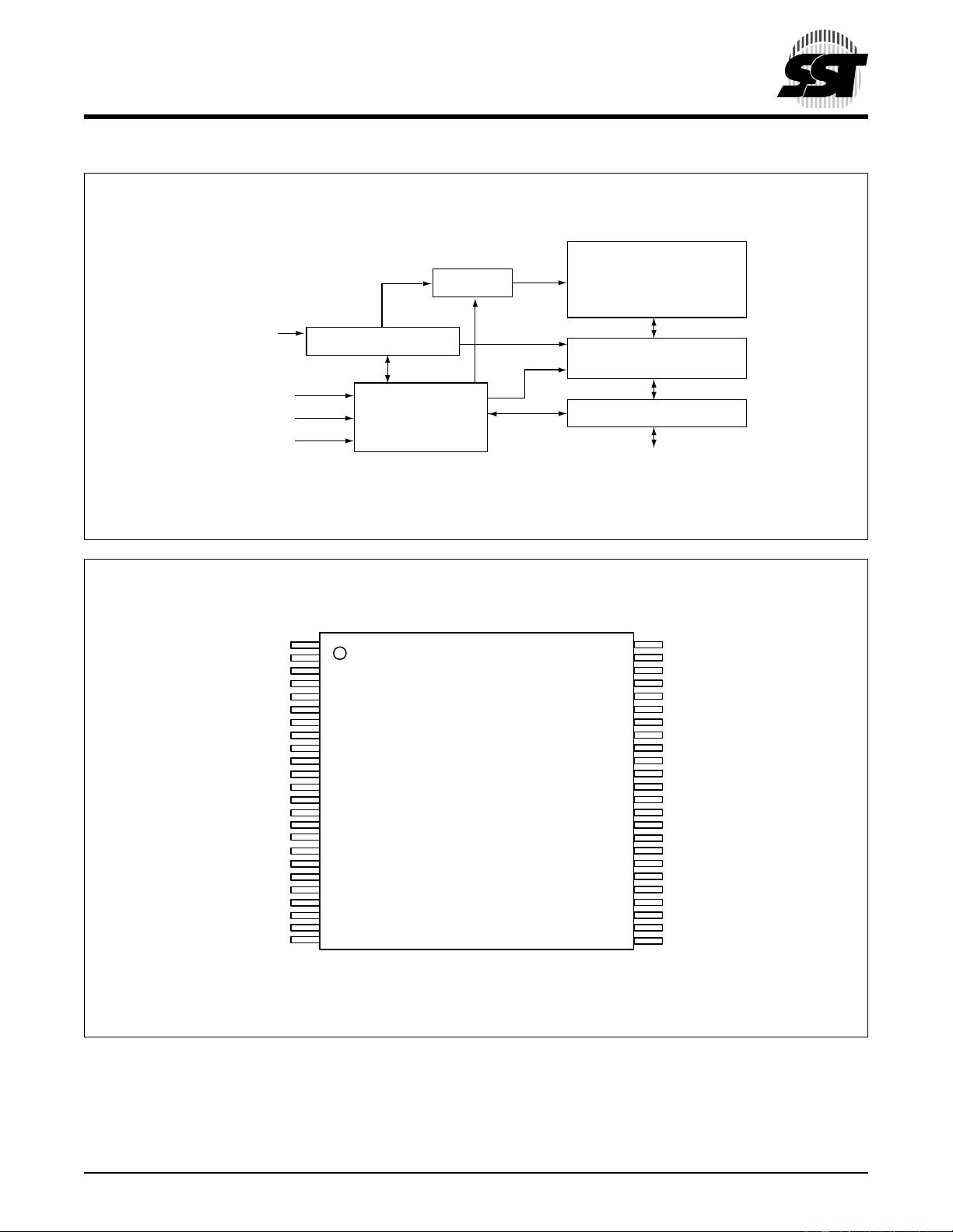
ages. See Figures 1 and 2 for pinouts.
2 Mbit / 4 Mbit / 8 Mbit (x16) Multi-Purpose Flash
SST39LF200A / SST39LF400A / SST39LF800A
SST39VF200A / SST39VF400A / SST39VF800A
SST39LF/VF200A / 400A / 800A3.0 & 2.7V 2Mb / 4Mb / 8Mb (x16) MPF memories
2
Data Sheet
2 Mbit / 4 Mbit / 8 Mbit Multi-Purpose Flash
SST39LF200A / SST39LF400A / SST39LF800A
SST39VF200A / SST39VF400A / SST39VF800A
©2001 Silicon Storage Technology, Inc. S71117-04-000 6/01 360
Device Operation
Commands are used to initiate the memory operation func-
tions of the device. Commands are written to the device
using standard microprocessor write sequences. A com-
mand is written by asserting WE# low while keeping CE#
low. The address bus is latched on the falling edge of WE#
or CE#, whichever occurs last. The data bus is latched on
the rising edge of WE# or CE#, whichever occurs first.
Read
The Read operation of the SST39LF200A/400A/800A and
SST39VF200A/400A/800A is controlled by CE# and OE#,
both have to be low for the system to obtain data from the
outputs. CE# is used for device selection. When CE# is
high, the chip is deselected and only standby power is con-
sumed. OE# is the output control and is used to gate data
from the output pins. The data bus is in high impedance
state when either CE# or OE# is high. Refer to the Read
cycle timing diagram for further details (Figure 3).
Word-Program Operation
The SST39LF200A/400A/800A and SST39VF200A/400A/
800A are programmed on a word-by-word basis. Before
programming, one must ensure that the sector, in which
the word which is being programmed exists, is fully erased.
The Program operation consists of three steps. The first
step is the three-byte load sequence for Software Data Pro-
tection. The second step is to load word address and word
data. During the Word-Program operation, the addresses
are latched on the falling edge of either CE# or WE#,
whichever occurs last. The data is latched on the rising
edge of either CE# or WE#, whichever occurs first. The
third step is the internal Program operation which is initi-
ated after the rising edge of the fourth WE# or CE#, which-
ever occurs first. The Program operation, once initiated, will
be completed within 20 µs. See Figures 4 and 5 for WE#
and CE# controlled Program operation timing diagrams
and Figure 16 for flowcharts. During the Program opera-
tion, the only valid reads are Data# Polling and Toggle Bit.
During the internal Program operation, the host is free to
perform additional tasks. Any commands issued during the
internal Program operation are ignored.
Sector/Block-Erase Operation
The Sector- (or Block-) Erase operation allows the system
to erase the device on a sector-by-sector (or block-by-
block) basis. The SST39LF200A/400A/800A and
SST39VF200A/400A/800A offers both Sector-Erase and
Block-Erase mode. The sector architecture is based on
uniform sector size of 2 KWord. The Block-Erase mode is
based on uniform block size of 32 KWord. The Sector-
Erase operation is initiated by executing a six-byte com-
mand sequence with Sector-Erase command (30H) and
sector address (SA) in the last bus cycle. The Block-Erase
operation is initiated by executing a six-byte command
sequence with Block-Erase command (50H) and block
address (BA) in the last bus cycle. The sector or block
address is latched on the falling edge of the sixth WE#
pulse, while the command (30H or 50H) is latched on the
rising edge of the sixth WE# pulse. The internal Erase
operation begins after the sixth WE# pulse. The End-of-
Erase operation can be determined using either Data#
Polling or Toggle Bit methods. See Figures 9 and 10 for tim-
ing waveforms. Any commands issued during the Sector-
or Block-Erase operation are ignored.
Chip-Erase Operation
The SST39LF200A/400A/800A and SST39VF200A/400A/
800A provide a Chip-Erase operation, which allows the
user to erase the entire memory array to the “1” state. This
is useful when the entire device must be quickly erased.
The Chip-Erase operation is initiated by executing a six-
byte command sequence with Chip-Erase command (10H)
at address 5555H in the last byte sequence. The Erase
operation begins with the rising edge of the sixth WE# or
CE#, whichever occurs first. During the Erase operation,
the only valid read is Toggle Bit or Data# Polling. See Table
4 for the command sequence, Figure 8 for timing diagram,
and Figure 19 for the flowchart. Any commands issued dur-
ing the Chip-Erase operation are ignored.
Write Operation Status Detection
The SST39LF200A/400A/800A and SST39VF200A/400A/
800A provide two software means to detect the completion
of a write (Program or Erase) cycle, in order to optimize the
system write cycle time. The software detection includes
two status bits: Data# Polling (DQ
7
) and Toggle Bit (DQ
6
).
The End-of-Write detection mode is enabled after the rising
edge of WE#, which initiates the internal Program or Erase
operation.
The actual completion of the nonvolatile write is asynchro-
nous with the system; therefore, either a Data# Polling or
Toggle Bit read may be simultaneous with the completion
of the write cycle. If this occurs, the system may possibly
get an erroneous result, i.e., valid data may appear to con-
flict with either DQ
7
or DQ
6
. In order to prevent spurious
rejection, if an erroneous result occurs, the software routine
should include a loop to read the accessed location an
additional two (2) times. If both reads are valid, then the
device has completed the write cycle, otherwise the rejec-
tion is valid.
Data Sheet
2 Mbit / 4 Mbit / 8 Mbit Multi-Purpose Flash
SST39LF200A / SST39LF400A / SST39LF800A
SST39VF200A / SST39VF400A / SST39VF800A
3
©2001 Silicon Storage Technology, Inc. S71117-04-000 6/01 360
Data# Polling (DQ
7
)
When the SST39LF200A/400A/800A and SST39VF200A/
400A/800A are in the internal Program operation, any
attempt to read DQ
7
will produce the complement of the
true data. Once the Program operation is completed, DQ
7
will produce true data. The device is then ready for the next
operation. During internal Erase operation, any attempt to
read DQ
7
will produce a ‘0’. Once the internal Erase opera-
tion is completed, DQ
7
will produce a ‘1’. The Data# Polling
is valid after the rising edge of fourth WE# (or CE#) pulse
for Program operation. For Sector-, Block- or Chip-Erase,
the Data# Polling is valid after the rising edge of sixth WE#
(or CE#) pulse. See Figure 6 for Data# Polling timing dia-
gram and Figure 17 for a flowchart.
Toggle Bit (DQ
6
)
During the internal Program or Erase operation, any con-
secutive attempts to read DQ
6
will produce alternating 1s
and 0s, i.e., toggling between 1 and 0. When the internal
Program or Erase operation is completed, the DQ
6
bit will
stop toggling. The device is then ready for the next opera-
tion. The Toggle Bit is valid after the rising edge of fourth
WE# (or CE#) pulse for Program operation. For Sector-,
Block- or Chip-Erase, the Toggle Bit is valid after the rising
edge of sixth WE# (or CE#) pulse. See Figure 7 for Toggle
Bit timing diagram and Figure 17 for a flowchart.
Data Protection
The SST39LF200A/400A/800A and SST39VF200A/400A/
800A provide both hardware and software features to pro-
tect nonvolatile data from inadvertent writes.
Hardware Data Protection
Noise/Glitch Protection: A WE# or CE# pulse of less than 5
ns will not initiate a write cycle.
V
DD
Power Up/Down Detection: The Write operation is
inhibited when V
DD
is less than 1.5V.
Write Inhibit Mode
: Forcing OE# low, CE# high, or WE#
high will inhibit the Write operation. This prevents inadvert-
ent writes during power-up or power-down.
Software Data Protection (SDP)
The SST39LF200A/400A/800A and SST39VF200A/400A/
800A provide the JEDEC approved Software Data Protec-
tion scheme for all data alteration operations, i.e., Program
and Erase. Any Program operation requires the inclusion of
the three-byte sequence. The three-byte load sequence is
used to initiate the Program operation, providing optimal
protection from inadvertent Write operations, e.g., during
the system power-up or power-down. Any Erase operation
requires the inclusion of six-byte sequence. This group of
devices are shipped with the Software Data Protection per-
manently enabled. See Table 4 for the specific software
command codes. During SDP command sequence, invalid
commands will abort the device to Read mode within TRC.
The contents of DQ
15
-DQ
8
can be V
IL
or V
IH
, but no other
value, during any SDP command sequence.
Common Flash Memory Interface (CFI)
The SST39LF200A/400A/800A and SST39VF200A/400A/
800A also contain the CFI information to describe the char-
acteristics of the device. In order to enter the CFI Query
mode, the system must write three-byte sequence, same
as Software ID Entry command with 98H (CFI Query com-
mand) to address 5555H in the last byte sequence. Once
the device enters the CFI Query mode, the system can
read CFI data at the addresses given in Tables 5 through 9.
The system must write the CFI Exit command to return to
Read mode from the CFI Query mode.
4
Data Sheet
2 Mbit / 4 Mbit / 8 Mbit Multi-Purpose Flash
SST39LF200A / SST39LF400A / SST39LF800A
SST39VF200A / SST39VF400A / SST39VF800A
©2001 Silicon Storage Technology, Inc. S71117-04-000 6/01 360
Product Identification
The Product Identification mode identifies the devices as
the SST39LF/VF200A, SST39LF/VF400A and SST39LF/
VF800A and manufacturer as SST. This mode may be
accessed by software operations. Users may use the
Software Product Identification operation to identify the part
(i.e., using the device ID) when using multiple
manufacturers in the same socket. For details, see Table 4
for software operation, Figure 11 for the Software ID Entry
and Read timing diagram, and Figure 18 for the Software
ID Entry command sequence flowchart.
Product Identification Mode Exit/
CFI Mode Exit
In order to return to the standard Read mode, the Software
Product Identification mode must be exited. Exit is accom-
plished by issuing the Software ID Exit command
sequence, which returns the device to the Read mode.
This command may also be used to reset the device to the
Read mode after any inadvertent transient condition that
apparently causes the device to behave abnormally, e.g.,
not read correctly. Please note that the Software ID Exit/
CFI Exit command is ignored during an internal Program or
Erase operation. See Table 4 for software command
codes, Figure 13 for timing waveform and Figure 18 for a
flowchart.
TABLE 1: P
RODUCT IDENTIFICATION TABLE
Address Data
Manufacturer’s ID 0000H 00BFH
Device ID
SST39LF/VF200A 0001H 2789H
SST39LF/VF400A 0001H 2780H
SST39LF/VF800A 0001H 2781H
T1.3 360
Data Sheet
2 Mbit / 4 Mbit / 8 Mbit Multi-Purpose Flash
SST39LF200A / SST39LF400A / SST39LF800A
SST39VF200A / SST39VF400A / SST39VF800A
5
©2001 Silicon Storage Technology, Inc. S71117-04-000 6/01 360
FIGURE 1: PIN ASSIGNMENTS FOR 48-LEAD TSOP
Y-Decoder
I/O Buffers and Data Latches
360 ILL B1.2
Address Buffer & Latches
X-Decoder
DQ
15
- DQ
0
Memory Address
OE#
CE#
WE#
SuperFlash
Memory
Control Logic
FUNCTIONAL BLOCK DIAGRAM
A15
A14
A13
A12
A11
A10
A9
A8
NC
NC
WE#
NC
NC
NC
NC
NC
NC
A7
A6
A5
A4
A3
A2
A1
1
2
3
4
5
6
7
8
9
10
11
12
13
14
15
16
17
18
19
20
21
22
23
24
A16
NC
V
SS
DQ15
DQ7
DQ14
DQ6
DQ13
DQ5
DQ12
DQ4
V
DD
DQ11
DQ3
DQ10
DQ2
DQ9
DQ1
DQ8
DQ0
OE#
V
SS
CE#
A0
48
47
46
45
44
43
42
41
40
39
38
37
36
35
34
33
32
31
30
29
28
27
26
25
360 ILL F01.2
Standard Pinout
Top View
Die Up
SST39LF200A/400A/800A
SST39VF200A/400A/800A
SST39LF/VF200A
A15
A14
A13
A12
A11
A10
A9
A8
NC
NC
WE#
NC
NC
NC
NC
NC
A17
A7
A6
A5
A4
A3
A2
A1
SST39LF/VF400A
A15
A14
A13
A12
A11
A10
A9
A8
NC
NC
WE#
NC
NC
NC
NC
A18
A17
A7
A6
A5
A4
A3
A2
A1
SST39LF/VF800A SST39LF/VF200A
A16
NC
V
SS
DQ15
DQ7
DQ14
DQ6
DQ13
DQ5
DQ12
DQ4
V
DD
DQ11
DQ3
DQ10
DQ2
DQ9
DQ1
DQ8
DQ0
OE#
V
SS
CE#
A0
SST39LF/VF400A
A16
NC
V
SS
DQ15
DQ7
DQ14
DQ6
DQ13
DQ5
DQ12
DQ4
V
DD
DQ11
DQ3
DQ10
DQ2
DQ9
DQ1
DQ8
DQ0
OE#
V
SS
CE#
A0
SST39LF/VF800A
剩余29页未读,继续阅读
资源评论
- demo02222013-03-25对我没多大作用
- bravecaicai2014-03-20好用的东西啊,太感谢啦
JYoung_
- 粉丝: 12
- 资源: 22
上传资源 快速赚钱
- 我的内容管理 展开
- 我的资源 快来上传第一个资源
- 我的收益 登录查看自己的收益
- 我的积分 登录查看自己的积分
- 我的C币 登录后查看C币余额
- 我的收藏
- 我的下载
- 下载帮助
安全验证
文档复制为VIP权益,开通VIP直接复制
信息提交成功