Page 2 of 224
KA49517A
Rev 1.02March 25, 2021
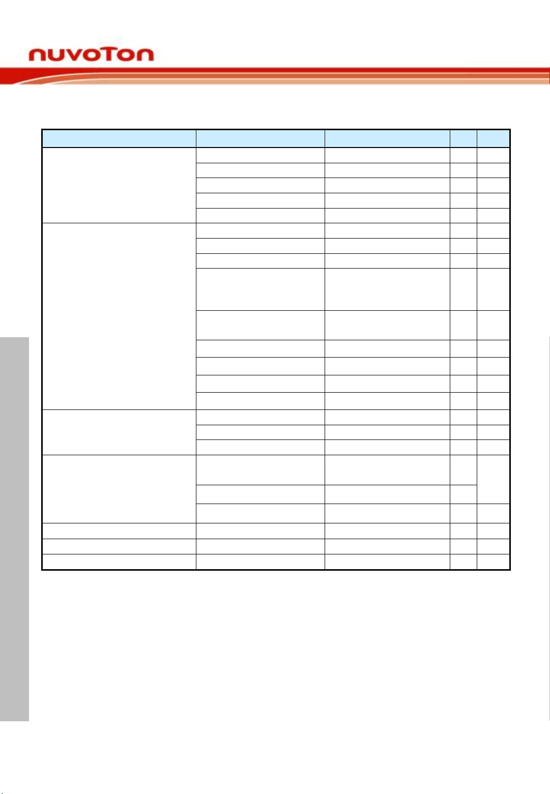
KA49517A Product Standards
Maximum support 17 battery cells in series
10mV measurement accuracy with 14 bits voltage ADC for cell
voltage, and 5 channels analog input measurement for
Thermistor
Built-in 16 bits Low speed Current measurement ADC
(Coulomb Counter) and 15 bits High speed Current
measurement ADC
Low–side Sense resistor Current measurement and monitoring
Operation mode - Active, Standby/Low power; Sleep and
Shutdown
SPI serial communication interface up to 1MHz clock with CRC
code correction and watchdog timer
Built-in ALARM pins for overvoltage, undervoltage, overcurrent
and short circuit detection and protection feature
Built-in cell balancing MOSFET, support external cell balance
MOSFET operation as well
3 channels General GPIO and 2 channels high voltage output
GPOH
Interrupt signal provision for MCU to notify state of operation as
well as measurement cycle indication at the available GPIO pins
High-side N-MOSFET driver: Charge (CHG) & Discharge (DIS)
with built-in charge pump and FETOFF control pin
Built in controllable fuse driver for cell OV and overcurrent
monitoring algorithm to serve as secondary protection system
Regulator (REG_EXT) for external circuit power provision with
selectable output setting 5V/3.3V/2.5V, and 50mA drive ability
Safety Diagnostic function for measurement related check and
FET driver check to enhance the total diagnostic coverage of
the chip
Package : TQFP 64L (10x10x1mm
3
, Lead Pitch 0.5mm)
System Block Diagram
Overview
KA49517A is a battery monitoring IC with protection function.
With high resolution ADC built-in, KA49517A is capable to
measure battery cell voltage and current level accurately.
Through SPI serial interface, microcontroller unit (MCU) is
able to read the status and measured result by KA49517A.
The ALARM pins alert the MCU with the abnormal condition
such as over voltage (OV), under voltage (UV),
over current (OC) and short circuit (SC).
KA49517A can support an application with up to 17 batteries
cells in series or a maximum voltage of 85V, it is suitable for
application with high input voltage such as E-bike, UPS etc.
Characteristics
• Pedelec, e-Bike, UPS, Server Backup System, Power Tool,
Energy Storage Systems etc
Applications
Notes: This is just an example of a circuit set: it is not guaranteed
to function identically to the final production version.
When designing a set for production, make sure to
carefully evaluate and verify the circuitry.
Representation Characteristics
Measurement accuracy
Application circuit example (17cells connection),
VBAT=62.9V , cell voltage ΔCn (C
n
-C
n-1
) = 3.7V
Measurement accuracy [mV]
Temperature [C]
SERIAL DATA
To and from
MCU/ECU
VBAT
GND
Reference
14bit
VADC
REGISTERS
AND
CONTROL
17-CELL
BATTERY
MUX
15 bit Fast
IADC
Reference
VPACK
FET Driver
16 bit Slow
IADC
Reference
VPACK+
VPACK-