Table Of Contents
- 3 -
IF THERE IS ANY OTHER OPERATION TO IMPLEMENT IN ADDITION TO SPECIFICATION
IN THE DATASHEET OR JEDEC STANDARD, PLEASE CONTACT EACH BRANCH OFFICE OR
HEADQUARTERS OF SAMSUNG ELECTRONICS.
datasheet
e·MMC
Preliminary Rev. 0.6
KLMxGxGEND-B031
SAMSUNG CONFIDENTIAL
1.0 PRODUCT LIST..........................................................................................................................................................4
2.0 KEY FEATURES.........................................................................................................................................................4
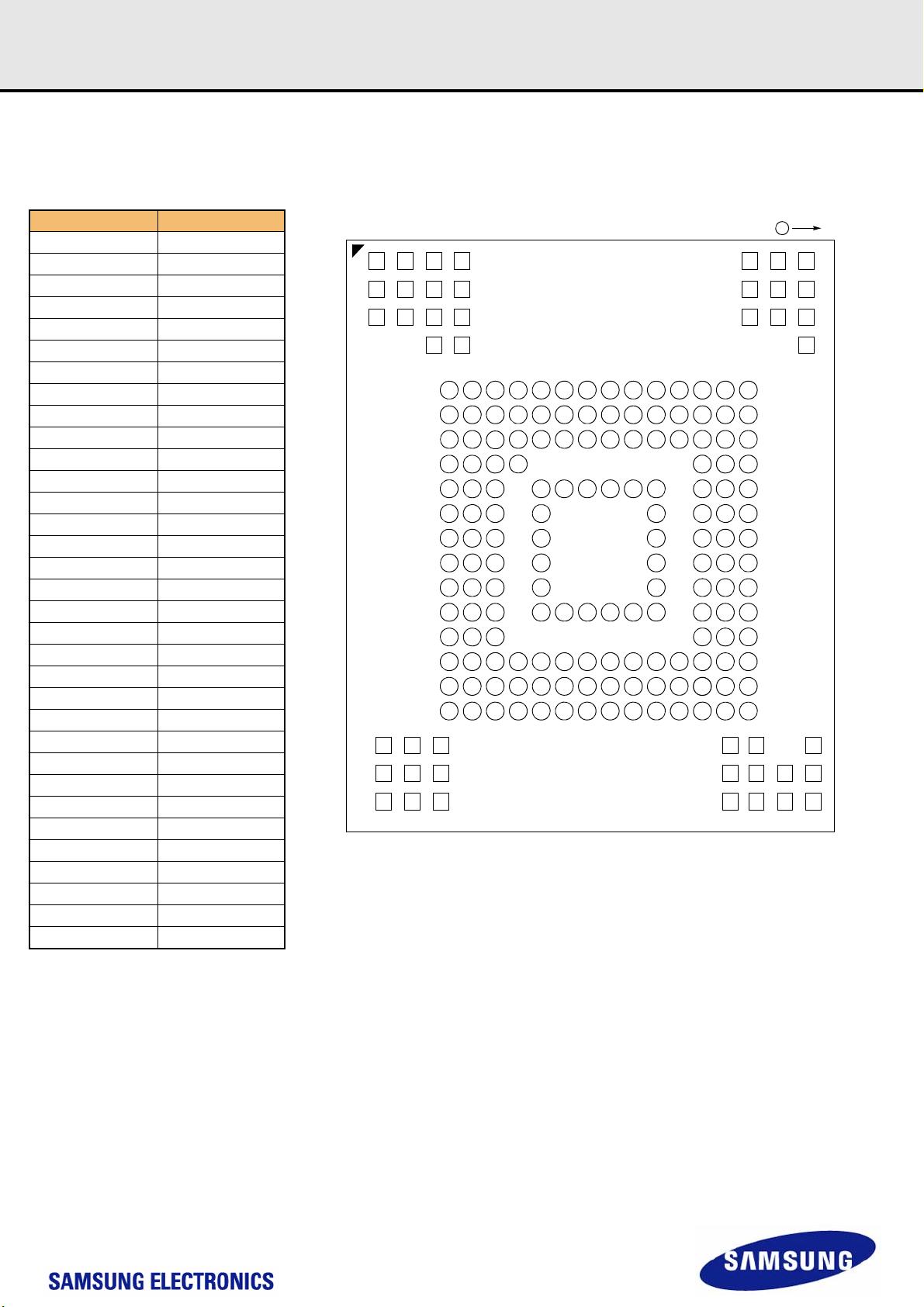
3.0 PACKAGE CONFIGURATIONS ................................................................................................................................. 5
3.1 153 Ball Pin Configuration ....................................................................................................................................... 5
3.1.1 11.5mm x 13mm x 0.8mm Package Dimension ............................................................................................... 6
3.1.2 11.5mm x 13mm x 1.0mm Package Dimension ............................................................................................... 6
3.2 Product Architecture ................................................................................................................................................ 7
4.0 e.MMC 5.0 feature ...................................................................................................................................................... 8
4.1 HS400 mode ........................................................................................................................................................... 8
5.0 Technical Notes ..........................................................................................................................................................10
5.1 S/W Agorithm .......................................................................................................................................................... 10
5.1.1 Partition Management ....................................................................................................................................... 10
5.1.1.1 Boot Area Partition and RPMB Area Partition ............................................................................................ 10
5.1.1.2 Enhanced Partition (Area) .......................................................................................................................... 10
5.1.2 Boot operation................................................................................................................................................... 11
5.1.3 User Density...................................................................................................................................................... 12
5.1.4 Auto Power Saving Mode.................................................................................................................................. 12
5.1.5 Performance...................................................................................................................................................... 12
6.0 REGISTER VALUE..................................................................................................................................................... 13
6.1 OCR Register .......................................................................................................................................................... 13
6.2 CID Register ............................................................................................................................................................ 13
6.2.1 Product name table (In CID Register) ............................................................................................................... 13
6.3 CSD Register........................................................................................................................................................... 14
6.4 Extended CSD Register .......................................................................................................................................... 15
7.0 AC PARAMETER........................................................................................................................................................ 20
7.1 Timing Parameter .................................................................................................................................................... 20
7.2 Previous Bus Timing Parameters for DDR52 and HS200 mode are defined by JEDEC standard.......................... 20
7.3 Bus Timing Specification in HS400 mode ............................................................................................................... 21
7.3.1 HS400 Device Input Timing .............................................................................................................................. 21
7.3.2 HS400 Device Output Timing............................................................................................................................ 22
7.4 Bus signal levels...................................................................................................................................................... 23
7.4.1 Open-drain mode bus signal level..................................................................................................................... 23
7.4.2 Push-pull mode bus signal level eMMC ............................................................................................................ 23
8.0 DC PARAMETER ...............................................................................................................
........................................ 24
8.1 Active Power Consumption during operation .......................................................................................................... 24
8.2 Standby Power Consumption in auto power saving mode and standby state........................................................ 24
8.3 Sleep Power Consumption in Sleep State.............................................................................................................. 24
8.4 Supply Voltage ........................................................................................................................................................ 24
8.5 Bus Signal Line Load............................................................................................................................................... 25