Modular Mid-Range PICmicro® KEELOQ® Decoder in C
需积分: 10 108 浏览量
2011-08-04
17:20:16
上传
评论
收藏 292KB PDF 举报

2001 Microchip Technology Inc. Preliminary DS00744A-page 1
M
AN744
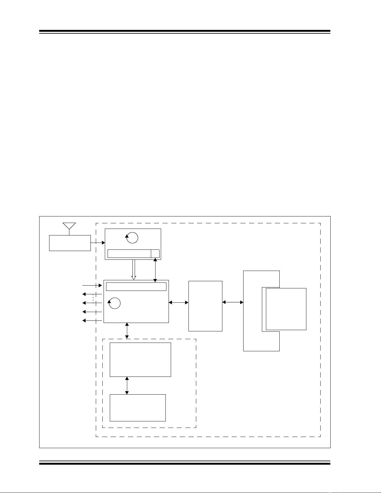
OVERVIEW
This application note describes a KEELOQ code hop-
ping decoder implemented on a Microchip Mid-range
Enhanced FLASH MCU (PIC16F872). The software
has been designed as a group of independent modules
(standard C source files "C" ).
For clarity and ease of maintenance, each module cov-
ers a single function. Each module can be modified to
accommodate a different behavior, support a different
MCU, and/or a different set of peripherals (memories,
timers, etc.).
KEY FEATURES
The set of modules presented in this application note
implement the following features:
• Source compatible with HITECH and CCS C
compilers
• Pin out compatible with PICDEM-2 board
• Normal Learn mode
• Learn up to 8 transmitters, using the internal
EEPROM memory of PIC16F872
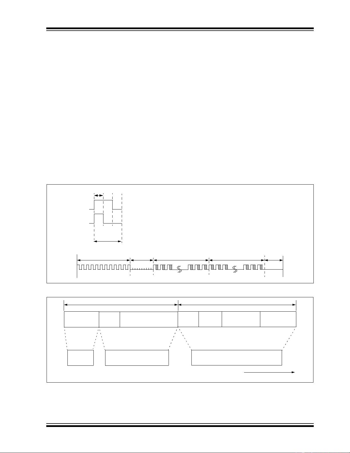
• Interrupt driven Radio Receive (PWM) routine
• Compatible with all existing K
EELOQ hopping code
encoders with PWM transmission format
selected, operating in "slow mode" (T
E = 400 µs)
• Automatic synchronization during receive, using a
4 MHz RC oscillator
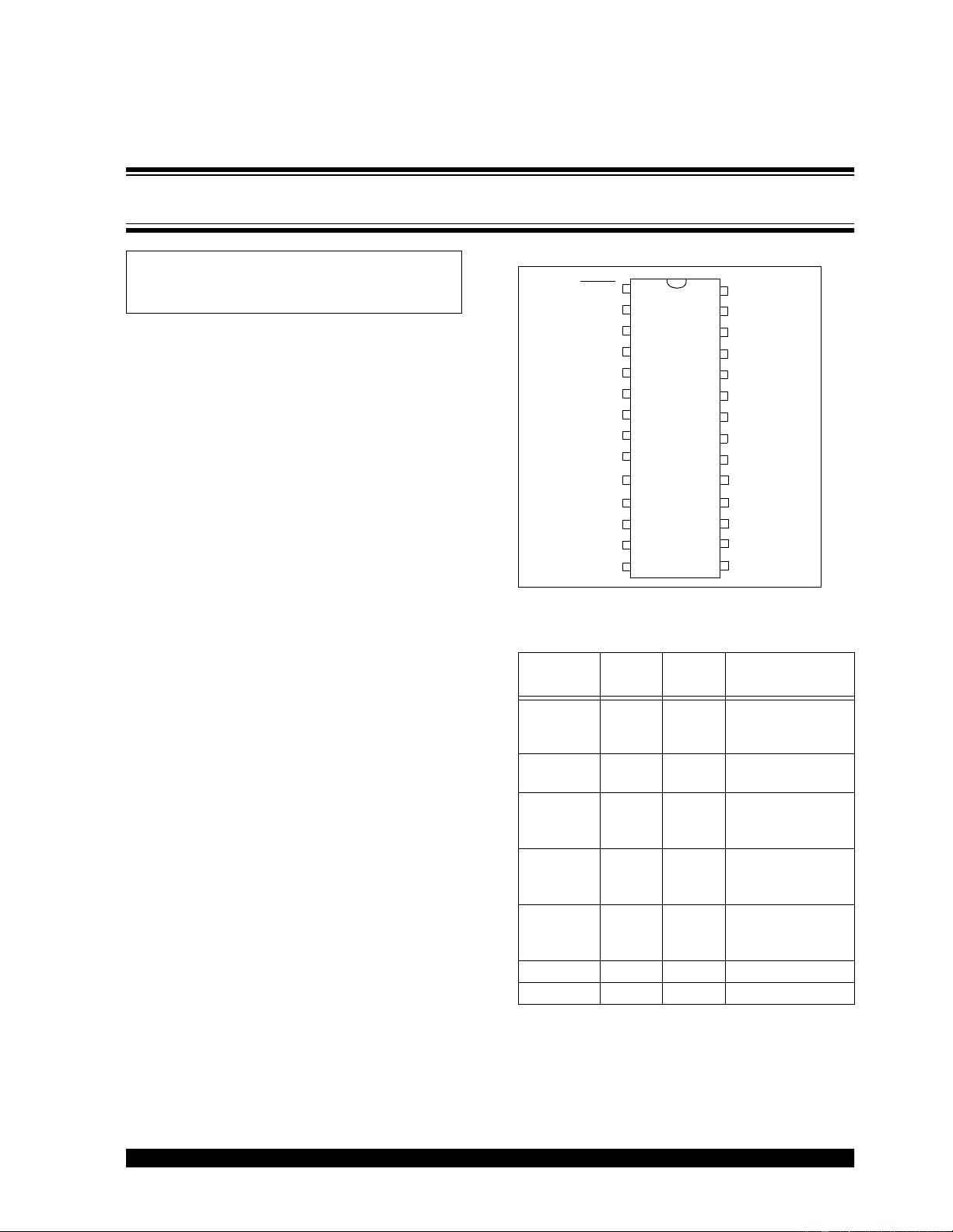
FIGURE 1: DECODER PIN OUT
TABLE 1: FUNCTIONAL INPUTS AND
OUTPUTS
Notice:
This is a non-restricted version of Application Note AN745 which is available under the K
EELOQ License
Agreement. The license agreement can be ordered from the Microchip Literature Center as DS40149.
Author: Lucio Di Jasio
Microchip Technology Inc.
Pin
Name
Pin
Number
Input/
Output
Function
RFIN 3 I Demodulated
PWM signal from
RF receiver
LEARN 6 I Input to enter learn
mode
LEARN-
OUT
25 O Output to show the
status of the learn
process
OUT0..3 21,22,2
3, 24
O Function outputs,
correspond to
encoder input pin
V
LOW 26 O Low Battery indica-
tor, as transmitted
by the encoder
VDD 20 PWR 5V power supply
VSS 19, 8 GND Common ground
Note: All NU pins are tristate
1
2
3
4
5
6
7
8
9
28
27
26
25
24
23
22
21
20
MCLR
LRNOUT
RF
IN
NU
NU
LEARN
NU
V
SS
OSCIN
NU
NU
V
LOW
LEARNOUT
OUT3
OUT2
OUT1
OUT0
V
DD
10
11
12
13
14
19
16
17
18
15
OSCOUT
NU
NU
NU
NU
V
SS
NU
NU
NU
NU
Modular Mid-Range PICmicro
®
KEELOQ
®
Decoder in C

剩余27页未读,继续阅读
资源评论


