Low Power, Low Dropout,
RF - Linear Regulators
2
SGM2019
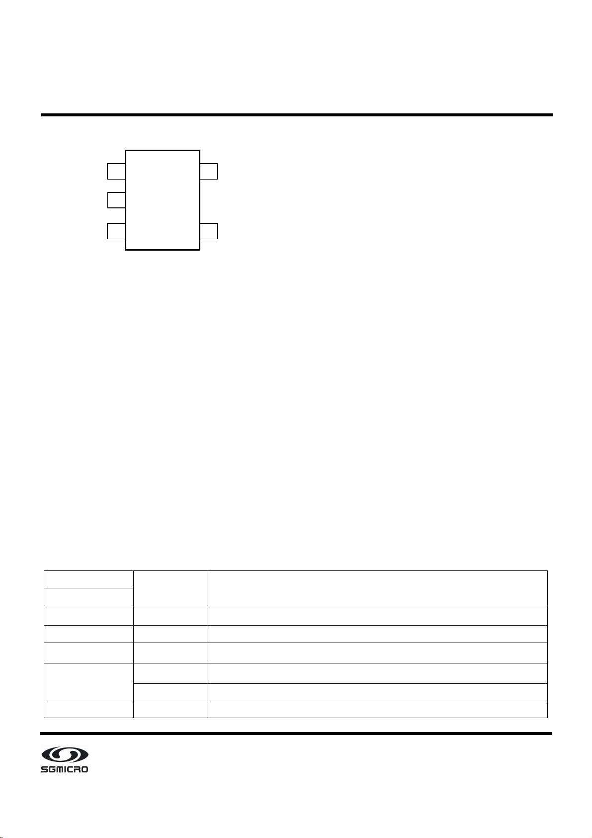
PIN CONFIGURATIONS (TOP VIEW)
1
2
3
4
5
OUT
IN
SOT-23-5/SC70-5
GND
EN
BP/FB
YJxx
NOTE:
1. The location of pin 1 on the YJxx is determined by orienting
the package marking as shown.
2. “xx” is the output voltage code. (For Example: when the
output voltage is 1.8V, it is expressed as 18.)
CAUTION
This integrated circuit can be damaged by ESD if you don’t pay
attention to ESD protection. SGMICRO recommends that all
integrated circuits be handled with appropriate precautions.
Failure to observe proper handling and installation procedures
can cause damage. ESD damage can range from subtle
performance degradation to complete device failure. Precision
integrated circuits may be more susceptible to damage because
very small parametric changes could cause the device not to
meet its published specifications.
SGMICRO reserves the right to make any change in circuit
design, specification or other related things if necessary without
notice at any time. Please contact SGMICRO sales office to get
the last datasheet.
ABSOLUTE MAXIMUM RATINGS
IN to GND................................................................ -0.3V to 6V
Output Short-Circuit Duration .........................................Infinite
EN to GND.............................................................. -0.3V to V
IN
OUT, BP/FB to GND.................................. -0.3V to (V
IN
+ 0.3V)
Power Dissipation, P
D
@ T
A
= 25℃
SOT-23-5......................................................................... 0.34W
SC70-5 ......................................................................... 0.175W
Package Thermal Resistance
SOT-23-5, θ
JA
.............................................................. 367℃/W
SC70-5, θ
JA
..................................................................710℃/W
Operating Temperature Range...........................-40℃ to +85℃
Junction Temperature...................................................... 150℃
Storage Temperature....................................... -65℃ to +150℃
Lead Temperature (soldering, 10s)..................................260℃
ESD Susceptibility
HBM................................................................................ 4000V
MM.................................................................................... 400V
NOTE:
Stresses beyond those listed under “Absolute Maximum
Ratings” may cause permanent damage to the device. These
are stress ratings only, and functional operation of the device
at these or any other conditions beyond those indicated in the
operational sections of the specifications is not implied.
Exposure to absolute maximum rating conditions for extended
periods may affect device reliability.
PIN DESCRIPTION
PIN
SC70-5 / SOT-23-5
NAME FUNCTION
1 IN
Regulator Input. Supply voltage can range from 2.5V to 5.5V. Bypass with a 1µF
capacitor to GND.
2 GND Ground.
3 EN
Shutdown Input. A logic low reduces the supply current to 10nA. Connect to IN for
normal operation.
BP
Reference-Noise Bypass (fixed voltage version only). Bypass with a low-leakage
0.01µF ceramic capacitor for reduced noise at the output.
4
FB Adjustable Voltage Version Only—this is used to set the output voltage of the device.
5 OUT Regulator Output.
代理商-联盛科技-0755-82514856 82514858
代理商-联盛科技-0755-82514856 82514858
评论0
最新资源