
Copyright 2017, KT Micro, Inc.
目录
Description .............................................................................................................................................. 1
1. Electrical Specification ............................................................................................................................ 4
2. Pin List .................................................................................................................................................... 7
3. Function Description ............................................................................................................................... 9
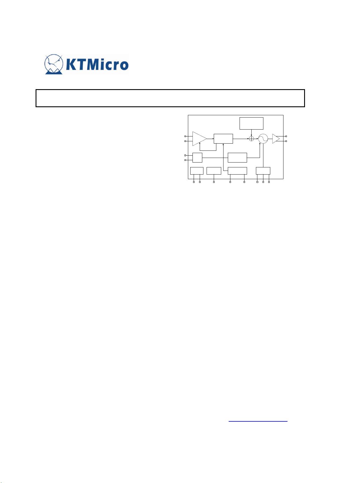
3.1. Overview ............................................................................................................................................. 9
3.2. Power-up and Standby ...................................................................................................................... 9
3.3. Crystal ................................................................................................................................................. 9
3.4. Microphone Interface .......................................................................................................................10
3.5. Audio AGC ........................................................................................................................................11
3.6. Audio ALC .........................................................................................................................................11
3.7. Audio equalization ............................................................................................................................15
3.8. Echo ....................................................................................................................................................15
3.9. Silence Mute and Audio signal detection ........................................................................................17
3.10. Pre emphasis ......................................................................................................................................17
3.11. Audio compressor ..............................................................................................................................17
3.12. Channel selection ...............................................................................................................................18
3.13. Transmission Power ..........................................................................................................................19
3.14. Digital Auxiliary Channel .................................................................................................................19
3.15. Battery voltage detection ..................................................................................................................19
3.16. 2-wire interface ..................................................................................................................................20
3.17. Register Bank ....................................................................................................................................22
3.17.1. MANUFACTURER_ID (Address 0x01) ......................................................................................22
3.17.2. BURST_DATA (Address 0x02) ...................................................................................................22
3.17.3. SYSCFG (Address 0x03) ..............................................................................................................22
3.17.4. BATTERY (Address 0x07) ...........................................................................................................22
3.17.5. CHAN_REGA (Address 0x08) .....................................................................................................22
3.17.6. CHAN_REGB (Address 0x09) .....................................................................................................22
3.17.7. CALI_CFG (Address 0x0A) .........................................................................................................23
3.17.8. PLL_STATE (Address 0x0D) .......................................................................................................23
3.17.9. POWER_CFG (Address 0x0F) .....................................................................................................23
3.17.10. PA_GAIN_CFG (Address 0x11) ..................................................................................................23
3.17.11. AUX_RESERVED_REG1 (Address 0x12) ..................................................................................23
3.17.12. AUX_RESERVED_REG2 (Address 0x13) ..................................................................................23
3.17.13. AUX_RESERVED_REG3 (Address 0x14) ..................................................................................24
3.17.14. TX_ID (Address 0x17) ..................................................................................................................24
3.17.15. DSP_CFGA (Address 0x1C) .........................................................................................................24
3.17.16. DSP_CFGC (Address 0x1E) .........................................................................................................25
3.17.17. PILOT_CFG (Address 0x1F) ........................................................................................................25
3.17.18. AUX_ADDR1 (Address 0x20) .....................................................................................................25
3.17.19. AUX_ADDR2 (Address 0x21) .....................................................................................................25
3.17.20. GPIO_CFG (Address 0x24) ..........................................................................................................26
3.17.21. SLNC_CFGA (Address 0x25) ......................................................................................................26
3.17.22. SLNC_CFGB (Address 0x26) .......................................................................................................27
3.17.23. AUX_RESERVED_REG4 (Address 0x27) ..................................................................................27
3.17.24. DSP_CFGB (Address 0x2B) .........................................................................................................28
3.17.25. DSP_PGA_CFGA(Address 0x30) ................................................................................................28
3.17.26. DSP_PGA_CFGB(Address 0x31) .................................................................................................28
3.17.27. DSP_ECHO_CFGA(Address 0x32)..............................................................................................29
3.17.28. DSP_EQ_CFGA(Address 0x34) ...................................................................................................29
3.17.29. DSP_EQ_CFGB (Address 0x35) ..................................................................................................31
3.17.30. DSP_EQ_CFGC (Address 0x36) ..................................................................................................32
3.17.31. DSP_EQ_CFGD (Address 0x37) ..................................................................................................34
3.17.32. DSP_EQ_CFGE (Address 0x38) ..................................................................................................35
3.17.33. DSP_HL_CP_CFG (Address 0x39) ..............................................................................................37
3.17.34. DSP_ALC_CFG (Address 0x3A) .................................................................................................38
3.17.35. STATUS_A (Address 0x3E) .........................................................................................................38
3.17.36. SPARE_A (Address 0x47) ............................................................................................................39
4. Typical Application Circuit ....................................................................................................................40


评论0