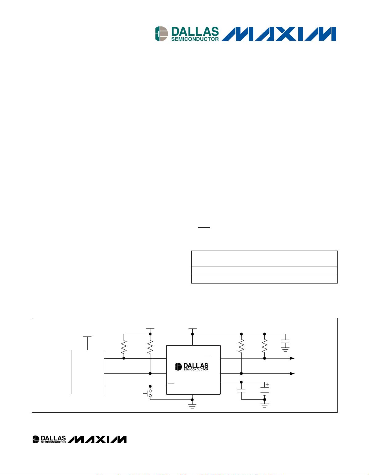
DS3231
高精度、
I
2
C
集成
RTC/TCXO/
晶体
2 _____________________________________________________________________
ABSOLUTE MAXIMUM RATINGS
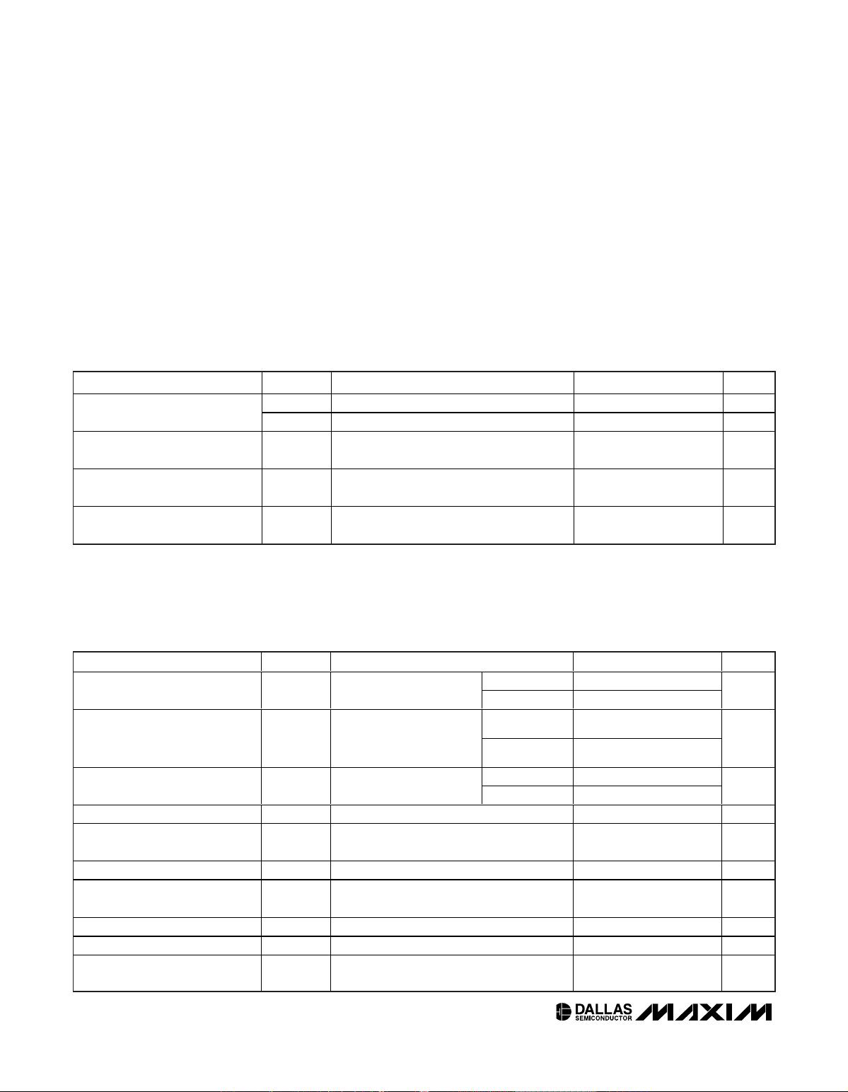
RECOMMENDED DC OPERATING CONDITIONS
(T
A
= T
MIN
to T
MAX
, unless otherwise noted.) (Notes 1, 2)
Stresses beyond those listed under “Absolute Maximum Ratings” may cause permanent damage to the device. These are stress ratings only, and functional
operation of the device at these or any other conditions beyond those indicated in the operational sections of the specifications is not implied. Exposure to
absolute maximum rating conditions for extended periods may affect device reliability.
Voltage Range on V
CC
, V
BAT
, 32kHz, SCL, SDA, RST,
INT/SQW Relative to Ground.............................-0.3V to +6.0V
Operating Temperature Range ...........................-40°C to +85°C
Junction Temperature......................................................+125°C
Storage Temperature Range ...............................-40°C to +85°C
Lead Temperature
(Soldering, 10s).....................................................+260°C/10s
Soldering Temperature....................................See the Handling,
PC Board Layout, and Assembly section.
PARAMETER SYMBOL CONDITIONS MIN TYP MAX UNITS
V
CC
2.3 3.3 5.5 V
Supply Voltage
V
BAT
2.3 3.0 5.5 V
Logic 1 Input SDA, SCL V
IH
0.7 x
V
CC
V
CC
+
0.3
V
Logic 0 Input SDA, SCL V
IL
-0.3
+0.3 x
V
CC
V
Pullup Voltage
(SDA, SCL, 32kHz, INT/SQW)
V
PU
V
CC
= 0V 5.5V V
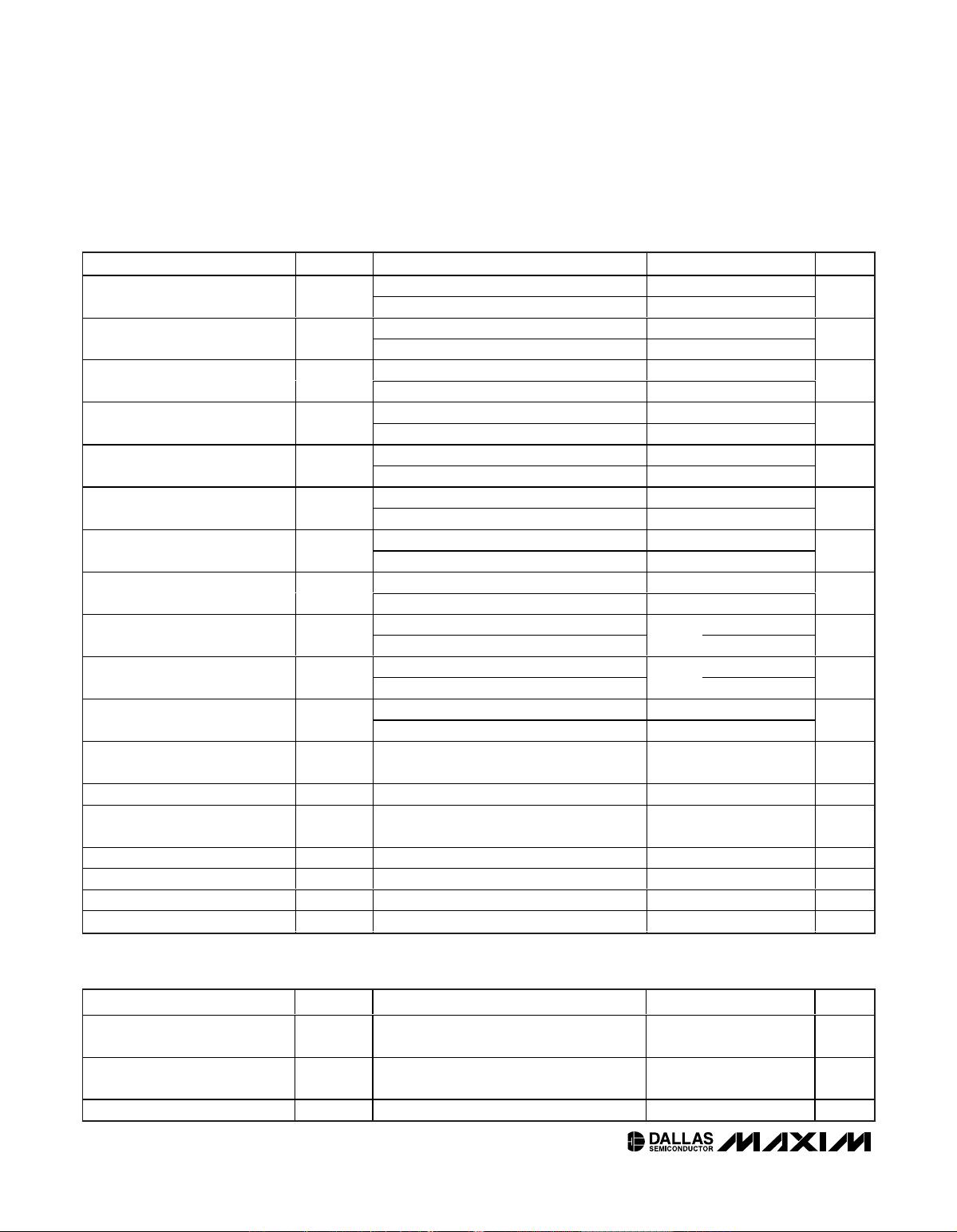
ELECTRICAL CHARACTERISTICS
(V
CC
= 2.3V to 5.5V, V
CC
> V
BAT
, T
A
= T
MIN
to T
MAX
, unless otherwise noted.) (Typical values are at V
CC
= 3.3V, V
BAT
= 3.0V, and
T
A
= +25°C, unless otherwise noted.) (Notes 1, 2)
PARAMETER SYMBOL CONDITIONS MIN TYP MAX UNITS
V
CC
= 3.63V 200
Active Supply Current I
CCA
(Notes 3, 4)
V
CC
= 5.5V 300
µA
V
CC
= 3.63V 110
Standby Supply Current I
CCS
I
2
C bus inactive, 32kHz
output on, SQW output off
(Note 4)
V
CC
= 5.5V 170
µA
V
CC
= 3.63V 575
Temperature Conversion Current I
CCSCONV
I
2
C bus inactive, 32kHz
output on, SQW output off
V
CC
= 5.5V 650
µA
Power-Fail Voltage V
PF
2.35 2.575 2.70 V
Logic 0 Output, 32kHz, INT/SQW,
SDA
V
OL
I
OL
= 3mA 0.4 V
Logic 0 Output, RST V
OL
I
OL
= 1mA 0.4 V
Output Leakage Current 32kHz,
INT/SQW, SDA
I
LO
Output high impedance -1 0 +1 µA
Input Leakage SCL I
LI
-1 +1 µA
RST Pin I/O Leakage I
OL
RST high impedance (Note 5) -200 +10 µA
V
BAT
Leakage Current
(V
CC
Active)
I
BATLKG
25 100 nA


