没有合适的资源?快使用搜索试试~ 我知道了~
资源详情
资源评论
资源推荐
![](https://csdnimg.cn/release/download_crawler_static/1900413/bg1.jpg)
© May 2009 Altera Corporation AN 367: Implementing PLL Reconfiguration in Stratix II Devices
AN-367-2.1
© May 2009
AN 367: Implementing PLL
Reconfiguration in Stratix II Devices
Introduction
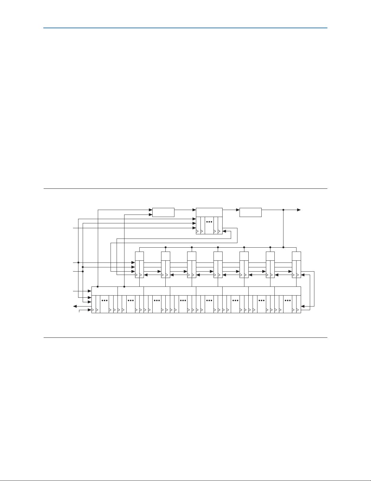
Phase-locked loops (PLLs) use several divide counters and different
voltage-controlled oscillator (VCO) phase taps to perform frequency synthesis and
phase shifts. In Stratix
®
II enhanced and fast PLLs, you can reconfigure both the
counter settings and phaseshift the PLL output clock in real time. You can also change
the charge pump and loop filter components, which dynamically affects the PLL
bandwidth. You can use these PLL components to update the output clock frequency,
PLL bandwidth, and phaseshift in real time, without reconfiguring the entire FPGA.
The ability to reconfigure the PLL in real time is useful in applications that might
operate at multiple frequencies. It is also useful in prototyping environments,
allowing you to sweep PLL output frequencies and adjust the output clock phase on
the fly. For instance, a system generating test patterns is required to generate and
transmit patterns at 50 or 100 MHz, depending on the device under test.
Reconfiguring the PLL components in real time allows you to switch between two
such output frequencies in a few microseconds. You can also use this feature to adjust
clock-to-out (t
CO
) delays in real time by changing output clock phase shift. This
approach eliminates the need to regenerate a configuration file with the new PLL
settings.
This application note discusses the following:
■ “PLL Reconfiguration Hardware Implementation” on page 2
■ “Reconfigurable Phase Shift” on page 8
■ “Charge Pump and Loop Filter” on page 10
■ “Bypassing PLL Counters” on page 13
■ “Implementing Reconfigurable PLLs in the Quartus II Software” on page 14
■ “PLL Configuration Scan Register Bit Map” on page 18
■ “Design Considerations” on page 22
■ “Phase Shift Stepping” on page 23
■ “Ports and Parameters” on page 25
■ “Reconfiguring the C0 Counter Using ALTPLL_RECONFIG” on page 29
■ “Design Examples” on page 31
![](https://csdnimg.cn/release/download_crawler_static/1900413/bg2.jpg)
Page 2 PLL Reconfiguration Hardware Implementation
AN 367: Implementing PLL Reconfiguration in Stratix II Devices © May 2009 Altera Corporation
PLL Reconfiguration Hardware Implementation
Enhanced and fast PLLs in Stratix II devices support real-time PLL reconfiguration.
The following PLL components are configurable in real time:
■ Pre-scale counter (n)
■ Feedback counter and VCO phase tap selection (m,
m
)
■ Post-scale output counters and VCO phase tap selection (C0 to C5,
C0
to
C5
)
■ Dynamically adjust the charge pump current (Icp), loop filter components (R, C) to
facilitate on the fly reconfiguration of the PLL bandwidth.
Figure 1 shows how PLL counter settings can be dynamically adjusted by shifting
their new settings into a serial shift register chain or scan chain. Serial data is input to
the scan chain via the scandata port and shift registers are clocked by scanclk. The
maximum scanclk frequency is 100 MHz. After the last bit of data is clocked,
asserting the scanwrite signal for at least one scanclk clock cycle causes the PLL
configuration bits to be synchronously updated with the data in the scan registers.
1 The counter and phase shift settings are updated synchronous to the clock frequency
of the individual counters. Therefore, all counters are not updated simultaneously.
Figure 1. PLL Reconfiguration Scan Chain (Note 1)
Note to Figure 1:
(1) The Stratix II fast PLLs do not support the C4 and C5 counters and the phase shift settings
C4
and
C5
.
/N /M /C0 /C1 /C2 /C3 /C4 /C5
scanclk
scandataout
scandata
CP/LF
scanread
scanwrite
inclk
PFD VCO
F
VCO
Φ
m
Φ
C0
Φ
C1
Φ
C2
Φ
C3
Φ
C4
Φ
C5
![](https://csdnimg.cn/release/download_crawler_static/1900413/bg3.jpg)
PLL Reconfiguration Hardware Implementation Page 3
© May 2009 Altera Corporation AN 367: Implementing PLL Reconfiguration in Stratix II Devices
Table 1 shows how these signals can be driven by the programmable logic device
(PLD) logic array or I/O pins.
All enhanced PLL counters except the m counter have 20 configuration bits. The m
counter has 22 configuration bits. Refer to Table 2 on page 5.
All fast PLL counters except the n counter have 12 configuration bits. The n counter
has 3 configuration bits. Refer to Table 3 on page 6.
There are two classes of counters, spread spectrum counters, and post-scale counters.
The following two subsections describe these counters.
Spread Spectrum Counters (m, n)
The enhanced PLL pre-scale counter, n, and feedback counter, m, implement spread
spectrum by switching between two different divide settings. These counters range
from 1 to 511. Therefore, the nominal count value and the spread spectrum count
value each need 9 configuration bits, for a total of 18 configuration bits. Two
additional configuration bits are used to bypass the nominal and spread counters (for
example, divide by 1). These two bypass bits must be set to the same value for proper
operation. This brings the total number of counter configuration bits to 20. When
spread spectrum is not used, the device uses the nominal count value and the spread
spectrum count value is ignored. The m counter uses an additional two configuration
bits to implement phase shift.
1 The Quartus
®
II software sets bits[9..0] for the m and n spread counter setting to
0000000000 if the spread spectrum feature is not used. If this feature is used, bits
[8..0] show the corresponding spread count value. The spread count bypass
setting, bit [9], is always set to 0.
Table 1. Real-Time PLL Reconfiguration Ports
PLL Port Name Description Source Destination
scandata Serial input data stream to scan chain. Logic array or I/O pins PLL reconfiguration
circuit
scanclk Serial clock input signal. This clock can be free
running.
Logic array or I/O pins PLL reconfiguration
circuit
scanwrite Writes the data in the scan chain to the PLL.
Active high.
Logic array or I/O pins PLL reconfiguration
circuit
scanread Enables scandata to be written into the scan
chain. Active high.
Logic array or I/O pins PLL reconfiguration
circuit
scandone Indicates when the PLL has finished
reprogramming. A rising edge indicates the PLL
has finished reprogramming.
PLL reconfiguration
circuit
Logic array or I/O pins
scandataout Used to output the contents of the scan chain. PLL reconfiguration
circuit
Logic array or I/O pins
![](https://csdnimg.cn/release/download_crawler_static/1900413/bg4.jpg)
Page 4 PLL Reconfiguration Hardware Implementation
AN 367: Implementing PLL Reconfiguration in Stratix II Devices © May 2009 Altera Corporation
Post-Scale Counters (C0 to C5)
The enhanced PLL, the C0 to C5 post-scale counters implement programmable duty
cycle and do not implement the spread spectrum feature. Refer to Figure 3 on page 6.
For enhanced PLLs, each counter has an 8-bit high time setting and an 8-bit low time
setting. The duty cycle is the ratio of output high or low time to the total cycle time,
which is the sum of the two. Additionally, these counters have two control bits,
rbypass, for bypassing the counter, and rselodd, to select the output clock duty
cycle, and two control bits for up/down phase shift selection, bringing the total
number of configuration bits to 20.
When the rbypass bit is set to 1, the PLL bypasses the counter, resulting in a divide
by 1. When this bit is set to 0, the high and low time counters are added to compute
the effective division of the VCO output frequency. For example, if the post-scale
divide factor is 10, the high and low count values could be set to 5 and 5 respectively,
to achieve a 50-50% duty cycle. The PLL implements this duty cycle by transitioning
the output clock from high to low on the rising edge of the VCO output clock.
However, a 4 and a 6 setting for the high and low count values, respectively, would
produce an output clock with 40-60% duty cycle.
The rselodd bit indicates an odd divide factor for the VCO output frequency along
with a 50% duty cycle. For example, if the post-scale divide factor was 3, the high and
low time count values could be set to 2 and 1 respectively to achieve this division.
This implies a 67%-33% duty cycle. If you need a 50%-50% duty cycle, you can set the
rselodd control bit to 1 to achieve this duty cycle despite an odd division factor. The
PLL implements this duty cycle by transitioning the output clock from high to low on
a falling edge of the VCO output clock. When you set rselodd = 1, you subtract 0.5
cycles from the high time and you add 0.5 cycles to the low time. For example:
■ High time count = 2 cycles
■ Low time count = 1 cycle
■ RSELODD = ‘1’ effectively equals:
■ High time count = 1.5 cycles
■ Low time count = 1.5 cycles
■ Duty cycle = (1.5/3) % high time count and (1.5/3) % low time count
Scan Chain Description
The length of the scan chain varies for different PLLs. Enhanced PLLs 5, 6, 11, and 12
have a 174-bit scan chain. Table 2 shows the number of bits for each component of the
enhanced PLL. Figure 2 shows the scan chain order of PLL components for enhanced
PLLs. Fast PLLs only have 6 counters and a 75-bit scan chain. Figure 5 on page 7
shows the scan chain order of each component for fast PLLs.
![](https://csdnimg.cn/release/download_crawler_static/1900413/bg5.jpg)
PLL Reconfiguration Hardware Implementation Page 5
© May 2009 Altera Corporation AN 367: Implementing PLL Reconfiguration in Stratix II Devices
Table 2 shows the scan registers for the counter settings that are marked n, m, and C0
to C5. Figure 1 on page 2 shows the scan registers for the phase shift markers that are
marked
m
,
C0
to
C5
.
Figure 2 shows the scan chain order of PLL components for enhanced PLLs 5, 6, 11,
and 12.
Table 2. Enhanced PLL Reprogramming Bits
Block Name
Number of Bits
Counter Phase Other (1) Total
C0 16 2 2 20
C1 16 2 2 20
C2 16 2 2 20
C3 16 2 2 20
C4 16 2 2 20
C5 16 2 2 20
M 182 222
N 180 220
Charge Pump0044
Loop Filter
Resistor
0066
Loop Filter
Capacitor
0022
Total number of bits 174
Note to Table 2:
(1) Includes two control bits, rbypass, for bypassing the counter, and rselodd, to select the output clock duty
cycle.
Figure 2. Scan Chain Order for Enhanced PLLs 5, 6, 11 and 12
φ
m
φ
C0
φ
C1
C4 C5 φ
C5
φ
C4
φ
C3
φ
C2
C3
C2 C1 C0
M N
Charge Pump/Loop Filter
LSB MSB
CP LF
DATAIN
DATAOUT
剩余31页未读,继续阅读
![pdf](https://img-home.csdnimg.cn/images/20210720083512.png)
![epub](https://img-home.csdnimg.cn/images/20210720083646.png)
![mobi](https://img-home.csdnimg.cn/images/20210720083646.png)
![pdf](https://img-home.csdnimg.cn/images/20210720083512.png)
![zip](https://img-home.csdnimg.cn/images/20210720083736.png)
![pdf](https://img-home.csdnimg.cn/images/20210720083512.png)
![azw3](https://img-home.csdnimg.cn/images/20210720083646.png)
![pdf](https://img-home.csdnimg.cn/images/20210720083512.png)
![application/pdf](https://img-home.csdnimg.cn/images/20210720083512.png)
![thumb](https://img-home.csdnimg.cn/images/20210720083646.png)
![epub](https://img-home.csdnimg.cn/images/20210720083646.png)
![pdf](https://img-home.csdnimg.cn/images/20210720083512.png)
![zip](https://img-home.csdnimg.cn/images/20210720083736.png)
![avatar](https://profile-avatar.csdnimg.cn/default.jpg!1)
asic1123
- 粉丝: 0
- 资源: 4
上传资源 快速赚钱
我的内容管理 展开
我的资源 快来上传第一个资源
我的收益
登录查看自己的收益我的积分 登录查看自己的积分
我的C币 登录后查看C币余额
我的收藏
我的下载
下载帮助
![voice](https://csdnimg.cn/release/downloadcmsfe/public/img/voice.245cc511.png)
![center-task](https://csdnimg.cn/release/downloadcmsfe/public/img/center-task.c2eda91a.png)
安全验证
文档复制为VIP权益,开通VIP直接复制
![dialog-icon](https://csdnimg.cn/release/downloadcmsfe/public/img/green-success.6a4acb44.png)
评论0