没有合适的资源?快使用搜索试试~ 我知道了~
XB8358D产品是锂离子/聚合物电池 保护的高集成解决方案 XB8358D0包 含先进的功率MOSFET,高
需积分: 0 1 下载量 12 浏览量
2024-04-22
16:15:33
上传
评论
收藏 1.22MB PDF 举报
温馨提示
试读
12页
该XB8358D产品是锂离子/聚合物电池保护的高集成解决方案。XB8358D0包 含先进的功率MOSFET,高精度电压检测电路和延迟电路。8358DO被放入一 个超小的SOT23-5封装,只有一个外部元件,使其成为理想的解决方案,在有 限的空间的电池组。XB8358D0具有电池应用所需的所有保护功能,包括过充 电,过放电,过电流和负载短路保护等。准确的过充电检测电压,确保充电安 全、充分利用。低待机电流在存储时从单元中消耗很少的电流。该设备不仅针 对数字化也可用于需要长期电池寿命的任何其它锂-隆和锂-聚合物电池供电的信息设 备。
资源推荐
资源详情
资源评论
XB8358D0
______________________________________ __________________________________ _______________ ________________
XySemi Inc - 1 - www.xysemi.com
REV0.3
One Cell Lithium-ion/Polymer Battery Protection IC
GENERAL DESCRIPTION
The XB8358D0 product is a high
integration solution for lithium-
ion/polymer battery protection.
XB8358D0 contains advanced power
MOSFET, high-accuracy voltage
detection circuits and delay circuits.
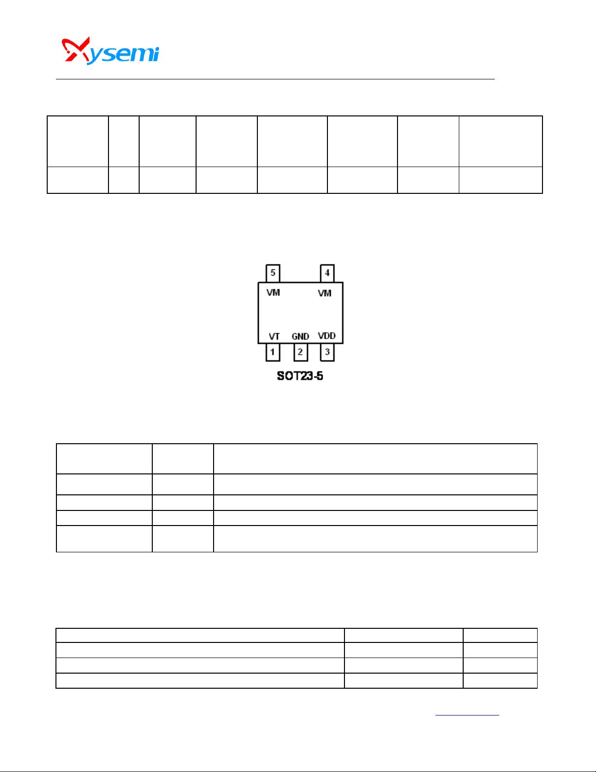
XB8358D0 is put into an ultra-small
SOT23-5 package and only one
external component makes it an ideal
solution in limited space of battery pack.
XB8358D0 has all the protection functions
required in the battery application including
overcharging, overdischarging, overcurrent
and load short circuiting protection etc. The
accurate overcharging detection voltage
ensures safe and full utilization charging.
The low standby current drains little current
from the cell while in storage.
The device is not only targeted for digital
cellular phones, but also for any other
Li-Ion and Li-Poly battery-powered
information appliances requiring long-
term battery life.
FEATURES
·
Protection of Charger Reverse
Connection
·
Protection of Battery Cell Reverse
Connection
·
Integrate Advanced Power MOSFET
with Equivalent of 45m
Ω
R
SS(ON)
·
Ultra-small SOT23-5 Package
·
Only One External Capacitor
Required
·
Over-temperature Protection
·
Overcharge Current Protection
·
Three-step Overcurrent Detection:
-Overdischarge Current 1
-Overdischarge Current 2
-Load Short Circuiting
·
Charger Detection Function
·
0V Battery Charging Function
- Delay Times are generated inside
·
High-accuracy Voltage Detection
·
Low Current Consumption
- Operation Mode: 2.8
μ
A typ.
- Power-down Mode: 1.5
μ
A typ.
·
RoHS Compliant and Lead (Pb) Free
APPLICATIONS
One-Cell Lithium-ion Battery Pack
Lithium-Polymer Battery Pack
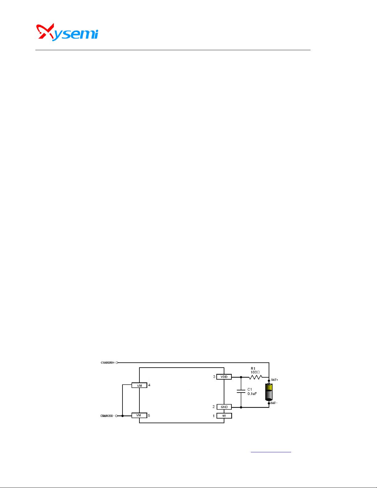
Figure 1. Typical Application Circuit
XB8358D0
______________________________________ ______________________ _________________________ _________________________
XySemi Inc - 2 - www.xysemi.com
REV0.3
ORDERING INFORMATION
PART
NUMBER
Pack
age
Overcharg
e Detection
Voltage
[VCU] (V)
Overcharge
Release
Voltage
[VCL] (V)
Overdischarge
Detection
Voltage
[VDL] (V)
Overdischarge
Release
Voltage
[VDR] (V)
Overcurrent
Detection
Current
[IOV1] (A)
Top Mark
XB8358D0
SOT
23-5
4.250
4.10
2.90
3.0
3.2
8358DYW(note)
Note: “YW” is manufacture date code, “Y” means the year, “W” means the week
PIN CONFIGURATION
Figure 2. PIN Configuration
PIN DESCRIPTION
XB8358D0 PIN
NUMBER
PIN NAME
PIN DESCRIPTION
1
V T
Test pin;only for vendor not used by application
2
GND
Ground, connect the negative terminal of the battery to this pin
3
VDD
Power Supply
4,5
VM
The negative terminal of the battery pack. The internal FET switch
connects this terminal to GND
ABSOLUTE MAXIMUM RATINGS
(Note: Do not exceed these limits to prevent damage to the device. Exposure to absolute maximum rating
conditions for long periods may affect device reliability.)
PARAMETER
VALUE
UNIT
VDD input pin voltage
-0.3 to 6
V
VM input pin voltage
-6 to 10
V
Operating Ambient Temperature
-40 to 85
°C
XB8358D0
______________________________________ ______________________ _________________________ _________________________
XySemi Inc - 3 - www.xysemi.com
REV0.3
Maximum Junction Temperature
125
°C
Storage Temperature
-55 to 150
°C
Lead Temperature ( Soldering, 10 sec)
300
°C
Power Dissipation at T=25°C
0.4
W
Package Thermal Resistance (Junction to Ambient)
θ
JA
250
°C /W
Package Thermal Resistance (Junction to Case)
θ
JC
130
°C /W
ESD
2000
V
ELECTRICAL CHARACTERISTICS
Typicals and limits appearing in normal type apply for T
A
= 25
o
C, unless otherwise specified
Parameter
Symbol
Test Condition
Min
Typ
Max
Unit
Detection Voltage
Overcharge Detection Voltage
V
CU
4.225
4.25
4.275
V
Overcharge Release Voltage
V
CL
4.075
4.10
4.125
V
Overdischarge Detection Voltage
V
DL
2.85
2.9
2.95
V
Overdischarge Release Voltage
V
DR
2.95
3.0
3.05
V
Charger Detection Voltage
V
CHA
-0.07
-0.12
-0.2
V
Detection Current
Overdischarge Current1 Detection
I
IOV1
V
DD
=3.5V
2.3
3.2
4.1
A
Load Short-Circuiting
Detection
I
SHORT
V
DD
=3.5V
10
20
30
A
Current Consumption
Current Consumption in Normal
Operation
I
OPE
V
DD
=3.5V
VM =0V
2.8
6
μ
A
Current Consumption in power
Down
I
PDN
V
DD
=2.0V
VM pin floating
1.5
μ
A
VM Internal Resistance
Internal Resistance between
VM and V
DD
R
VMD
V
DD
=3.5V
VM=1.0V
320
k
Ω
Internal Resistance between VM
and GND
R
VMS
V
DD
=2.0V
VM=1.0V
100
k
Ω
FET on Resistance
30
Equivalent FET on Resistance
R
SS(ON)
V
DD
=3.6V I
VM
=1.0A
45
m
Ω
Over Temperature Protection
120
Over Temperature Protection
T
SHD+
120
剩余11页未读,继续阅读
资源评论
奥科迪科技13480937849
- 粉丝: 196
- 资源: 12
上传资源 快速赚钱
- 我的内容管理 展开
- 我的资源 快来上传第一个资源
- 我的收益 登录查看自己的收益
- 我的积分 登录查看自己的积分
- 我的C币 登录后查看C币余额
- 我的收藏
- 我的下载
- 下载帮助
安全验证
文档复制为VIP权益,开通VIP直接复制
信息提交成功