


NUC970 Technical Reference Manual
Publication Release Date: Sept. 24, 2015
- 1 - Revision V1.20
NUC970 TECHNICAL REFERENCE MANUAL
ARM926EJ-S Based
32-bit Microcontroller
NUC970 Series
Technical Reference Manual
The information described in this document is the exclusive intellectual property of
Nuvoton Technology Corporation and shall not be reproduced without permission from Nuvoton.
Nuvoton is providing this document only for reference purposes of NuMicro microcontroller based
system design. Nuvoton assumes no responsibility for errors or omissions.
All data and specifications are subject to change without notice.
For additional information or questions, please contact: Nuvoton Technology Corporation.
www.nuvoton.com

NUC970 Technical Reference Manual
Publication Release Date: Sept. 24, 2015
- 2 - Revision V1.20
NUC970 TECHNICAL REFERENCE MANUAL
TABLE OF CONTENTS
TABLE OF CONTENTS ......................................................................... 2
LIST OF FIGURES ............................................................................. 11
LIST OF TABLES .............................................................................. 16
1 GENERAL DESCRIPTION ............................................................ 17
2 FEATURES .............................................................................. 18
NUC970 Series Features ................................................................... 18 2.1
3 PARTS INFORMATION LIST AND PIN CONFIGURATION ..................... 25
NUC970 Series Part Number Naming Guide............................................ 25 3.1
NUC970 Series Part Selection Guide .................................................... 26 3.2
Pin Configuration ............................................................................. 28 3.3
3.3.1 NUC972DFxxY Pin Diagram ...................................................................... 28
3.3.2 NUC973DFxxY Pin Diagram ...................................................................... 29
3.3.3 NUC976DKxxY Pin Diagram ...................................................................... 30
3.3.4 NUC977DKxxY Pin Diagram ...................................................................... 31
3.3.5 NUC978YOxxY Pin Diagram ..................................................................... 32
Pin Description ............................................................................... 33 3.4
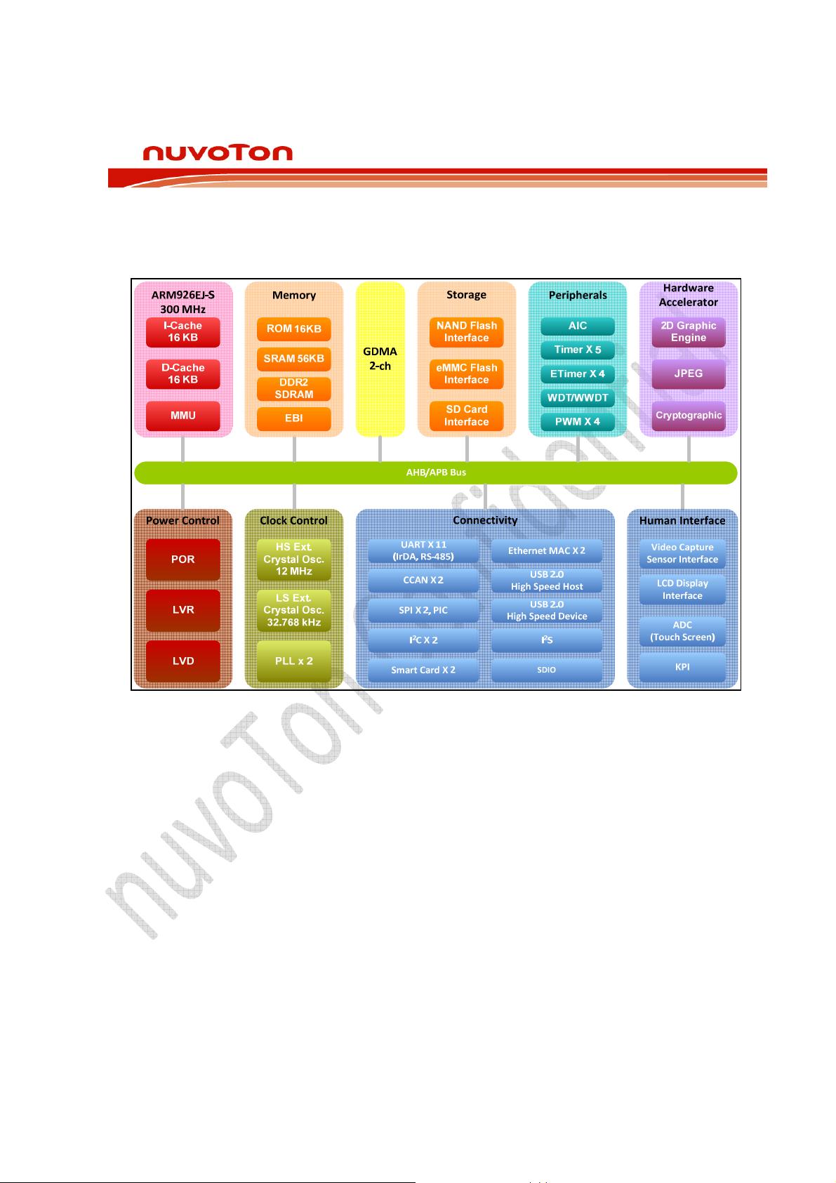
4 BLOCK DIAGRAM ...................................................................... 59
NUC970 Series Block Diagram ............................................................ 59 4.1
5 FUNCTIONAL DESCRIPTION ........................................................ 60
ARM
®
ARM926EJ-S CPU Core ........................................................... 60 5.1
5.1.1 Overview ............................................................................................. 60
5.1.2 System Control Coprocessor (CP15) ............................................................ 61
5.1.3 Memory Management Unit (MMU) ............................................................... 61
5.1.4 Caches and Write Buffer ........................................................................... 62
5.1.5 Bus Interface Unit ................................................................................... 63
5.1.6 Power Management ................................................................................ 63
System Manager ............................................................................. 64 5.2
5.2.1 Overview ............................................................................................. 64
5.2.2 System Reset........................................................................................ 64
5.2.3 System Power Distribution ........................................................................ 65
5.2.4 System Memory Map ............................................................................... 66
5.2.5 Power-On Setting ................................................................................... 70

NUC970 Technical Reference Manual
Publication Release Date: Sept. 24, 2015
- 3 - Revision V1.20
NUC970 TECHNICAL REFERENCE MANUAL
5.2.6 Register Map ........................................................................................ 72
5.2.7 Register Description ................................................................................ 74
Clock Controller (CLK_CTL) ............................................................. 140 5.3
5.3.1 Overview ........................................................................................... 140
5.3.2 Features ............................................................................................ 140
5.3.3 Block diagram ..................................................................................... 141
5.3.4 Functional description ............................................................................ 150
5.3.5 Registers Map ..................................................................................... 152
5.3.6 Register description .............................................................................. 153
Advanced Interrupt Controller (AIC) .................................................... 187 5.4
5.4.1 Overview ........................................................................................... 187
5.4.2 Features ............................................................................................ 187
5.4.3 Block Diagram ..................................................................................... 188
5.4.4 Functional Description ........................................................................... 188
5.4.5 Register Map ...................................................................................... 193
5.4.6 Register Description .............................................................................. 195
SDRAM Interface Controller (SDIC) .................................................... 218 5.5
5.5.1 Overview ........................................................................................... 218
5.5.2 Features ............................................................................................ 218
5.5.3 Block Diagram ..................................................................................... 219
5.5.4 Basic Configuration ............................................................................... 220
5.5.5 Functional Description ........................................................................... 220
5.5.6 Register Map ...................................................................................... 224
5.5.7 Register Description .............................................................................. 224
MTP Controller (MTP) ..................................................................... 246 5.6
5.6.1 Overview ........................................................................................... 246
5.6.2 Features ............................................................................................ 246
5.6.3 Block Diagram ..................................................................................... 247
5.6.4 Basic Configuration ............................................................................... 248
5.6.5 Software Programming Flow .................................................................... 249
5.6.6 Register Map ...................................................................................... 250
5.6.7 Register Description .............................................................................. 251
External Bus Interface (EBI) ............................................................. 260 5.7
5.7.1 Overview ........................................................................................... 260
5.7.2 Features ............................................................................................ 260
NUC970 Technical Reference Manual
Publication Release Date: Sept. 24, 2015
- 4 - Revision V1.20
NUC970 TECHNICAL REFERENCE MANUAL
5.7.3 Block Diagram ..................................................................................... 260
5.7.4 Basic Configuration ............................................................................... 261
5.7.5 Functional Description ........................................................................... 261
5.7.6 Register Map ...................................................................................... 262
5.7.7 Register Description .............................................................................. 263
General Purpose I/O (GPIO) ............................................................. 271 5.8
5.8.1 Overview ........................................................................................... 271
5.8.2 Features ............................................................................................ 271
5.8.3 Block Diagram ..................................................................................... 271
5.8.4 Basic Configuration ............................................................................... 272
5.8.5 Functional Description ........................................................................... 272
5.8.6 Register Map ...................................................................................... 272
5.8.7 Register Description .............................................................................. 277
General DMA Controller (GDMA) ....................................................... 297 5.9
5.9.1 Overview ........................................................................................... 297
5.9.2 Features ............................................................................................ 297
5.9.3 Block Diagram ..................................................................................... 297
5.9.4 Basic Configuration ............................................................................... 298
5.9.5 Functional Description ........................................................................... 298
5.9.6 Register Map ...................................................................................... 302
5.9.7 Register Description .............................................................................. 303
Timer Controller (TMR) ................................................................... 320 5.10
5.10.1 Overview ........................................................................................ 320
5.10.2 Features ......................................................................................... 320
5.10.3 Block Diagram .................................................................................. 321
5.10.4 Basic Configuration ............................................................................ 321
5.10.5 Functional Description ......................................................................... 321
5.10.6 Register Map.................................................................................... 323
5.10.7 Register Description ........................................................................... 324
Enhance Timer Controller (ETMR) ...................................................... 330 5.11
5.11.1 Overview ........................................................................................ 330
5.11.2 Features ......................................................................................... 330
5.11.3 Block Diagram .................................................................................. 330
5.11.4 Basic Configuration ............................................................................ 331
5.11.5 Functional Description ......................................................................... 331
NUC970 Technical Reference Manual
Publication Release Date: Sept. 24, 2015
- 5 - Revision V1.20
NUC970 TECHNICAL REFERENCE MANUAL
5.11.6 Register Map.................................................................................... 334
5.11.7 Register Description ........................................................................... 334
Pulse Width Modulation (PWM) ......................................................... 345 5.12
5.12.1 Overview ........................................................................................ 345
5.12.2 Features ......................................................................................... 345
5.12.3 Block Diagram .................................................................................. 346
5.12.4 Basic Configuration ............................................................................ 346
5.12.5 Functional Description ......................................................................... 346
5.12.6 Register Map.................................................................................... 350
5.12.7 Register Description ........................................................................... 351
Watchdog Timer (WDT)................................................................... 361 5.13
5.13.1 Overview ........................................................................................ 361
5.13.2 Features ......................................................................................... 361
5.13.3 Block Diagram .................................................................................. 361
5.13.4 Basic Configuration ............................................................................ 361
5.13.5 Functional Description ......................................................................... 362
5.13.6 Register Map.................................................................................... 365
5.13.7 Register Description ........................................................................... 366
Windowed Watchdog Timer (WWDT) .................................................. 370 5.14
5.14.1 Overview ........................................................................................ 370
5.14.2 Features ......................................................................................... 370
5.14.3 Block Diagram .................................................................................. 370
5.14.4 Basic Configuration ............................................................................ 370
5.14.5 Function Description ........................................................................... 371
5.14.6 Register Map.................................................................................... 375
5.14.7 Register Description ........................................................................... 376
Real Time Clock (RTC) ................................................................... 382 5.15
5.15.1 Overview ........................................................................................ 382
5.15.2 Features ......................................................................................... 382
5.15.3 Block Diagram .................................................................................. 383
5.15.4 Basic Configuration ............................................................................ 383
5.15.5 Functional Description ......................................................................... 383
5.15.6 Register Map.................................................................................... 385
5.15.7 Register Description ........................................................................... 387
UART Interface Controller (UART) ...................................................... 409 5.16


评论1