89c51单片机 英语文献翻译.doc

信息与控制
英文原文
Description
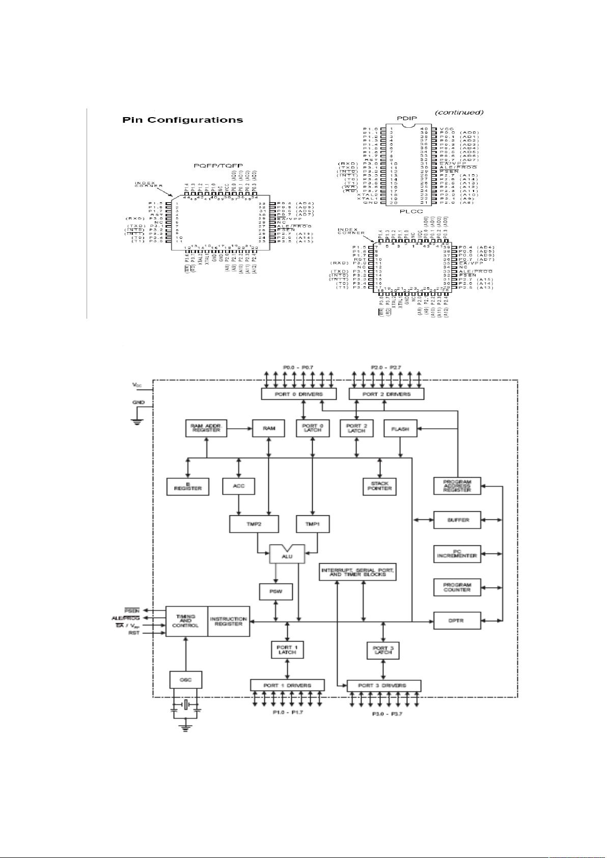
The AT89C51 is a low-power, high-performance CMOS 8-bit microcomputer with 4K bytes of
Flash Programmable and Erasable Read Only Memory (PEROM) and 128 bytes RAM. The device is
manufactured using Atmel’s high density nonvolatile memory technology and is compatible with the
industry standard MCS-51™ instruction set and pinout. The chip combines a versatile 8-bit CPU with
Flash on a monolithic chip, the Atmel AT89C51 is a powerful microcomputer which provides a highly
flexible and cost effective solution to many embedded control applications.
Features:
• Compatible with MCS-51™ Products
• 4K Bytes of In-System Reprogrammable Flash Memory
• Endurance: 1,000 Write/Erase Cycles
• Fully Static Operation: 0 Hz to 24 MHz
• Three-Level Program Memory Lock
• 128 x 8-Bit Internal RAM
• 32 Programmable I/O Lines
• Two 16-Bit Timer/Counters
• Six Interrupt Sources
• Programmable Serial Channel
• Low Power Idle and Power Down Modes
The AT89C51 provides the following standard features: 4K bytes of Flash, 128 bytes of RAM, 32
I/O lines, two 16-bit timer/counters, a five vector two-level interrupt architecture, a full duplex serial
port, on-chip oscillator and clock circuitry. In addition, the AT89C51 is designed with static logic for
operation down to zero frequency and supports two software selectable power saving modes. The Idle
Mode stops the CPU while allowing the RAM, timer/counters, serial port and interrupt system to
continue functioning. The Power Down Mode saves the RAM contents but freezes the oscillator
disabling all other chip functions until the next hardware reset.


剩余31页未读,继续阅读


评论1
最新资源