没有合适的资源?快使用搜索试试~ 我知道了~
资源推荐
资源详情
资源评论
DS791 June 22, 2011 www.xilinx.com 1
Product Specification
© Copyright 2010-2011. Xilinx, Inc. Xilinx, Inc. Xilinx, the Xilinx logo, Artix, ISE, Kintex, Spartan, Virtex, Zynq, and other designated brands included herein are
trademarks of Xilinx in the United States and other countries. ARM is a registered trademark of ARM in the EU and other countries. The AMBA trademark is a
registered trademark of ARM Limited. All other trademarks are the property of their respective owners.
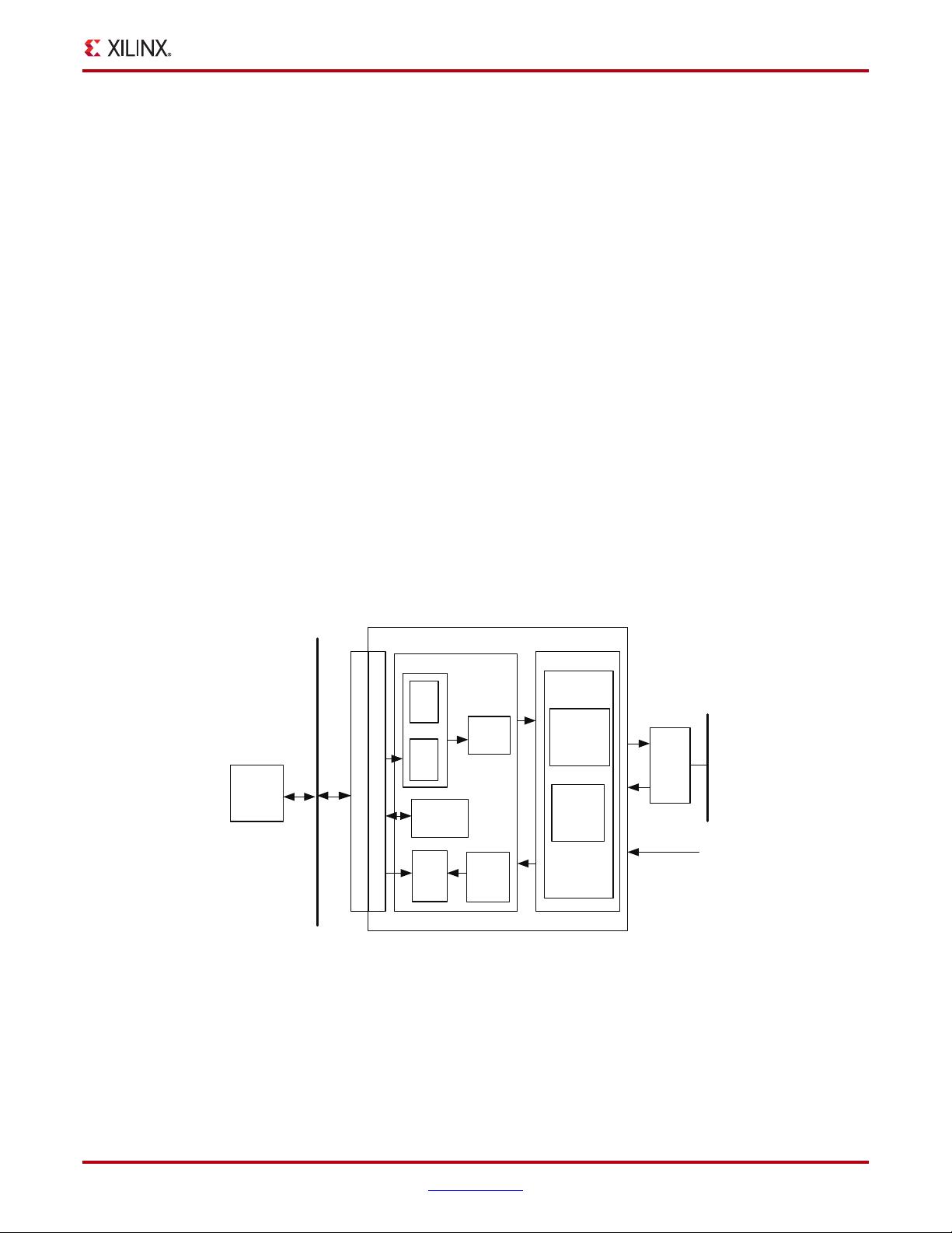
Introduction
The Xilinx® LogiCORE™ IP Controller Area Network
(CAN) product specification defines the architecture
and features of the Xilinx CAN controller core. This
document also defines the addressing and functionality
of the various registers in the design, in addition to
describing the user interface. The scope of this
document does not extend to describing the CAN
protocol and assumes knowledge of the specifications
described in the Reference Documents section.
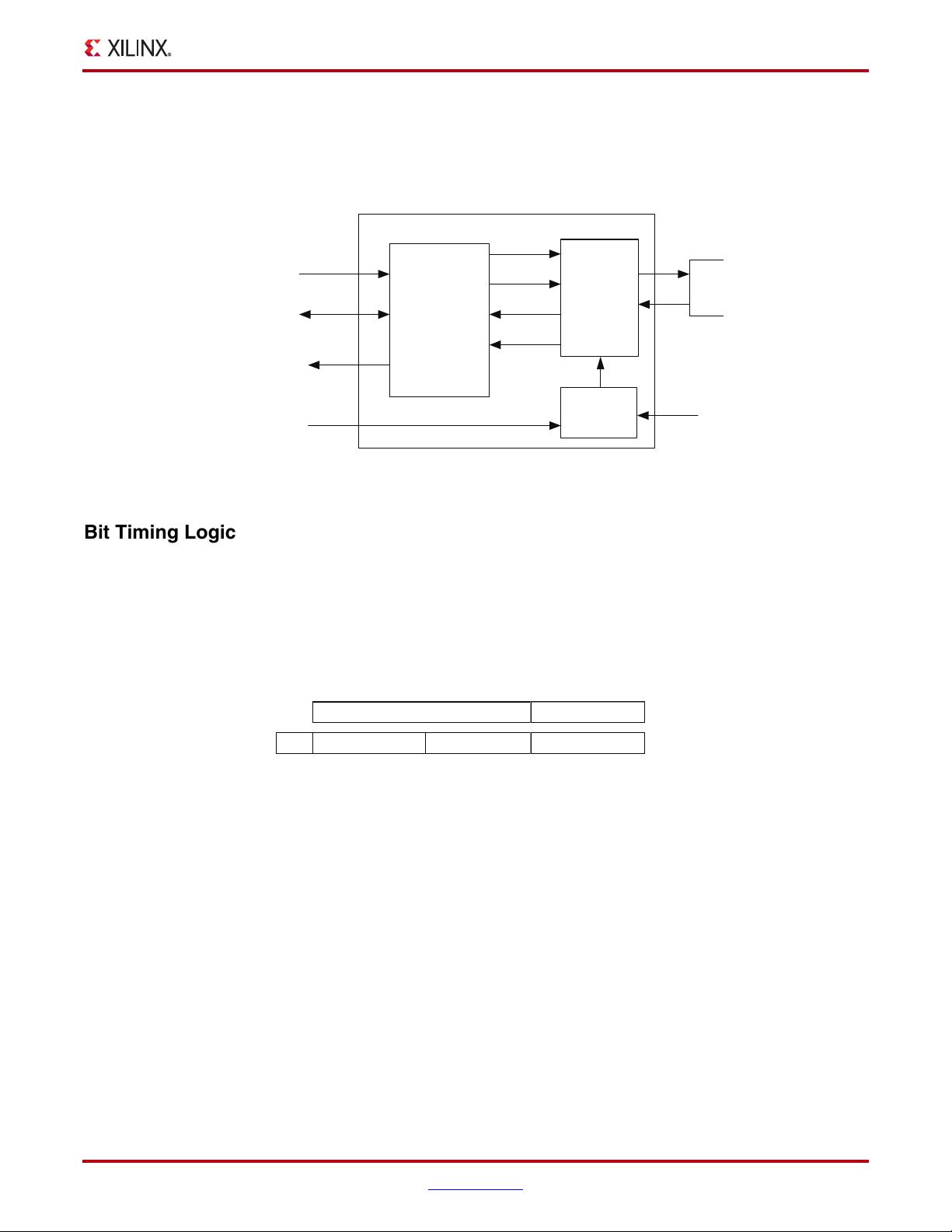
Features
• Conforms to the ISO 11898 -1, CAN 2.0A, and CAN
2.0B standards
• Supports Industrial (I) and Extended Temperature
Range (Q) grade device support
• Supports both standard (11-bit identifier) and
extended (29-bit identifier) frames
• Supports bit rates up to 1 Mb/s
• Transmit message FIFO with a user-configurable
depth of up to 64 messages
• Transmit prioritization through one High-Priority
Transmit buffer
• Automatic re-transmission on errors or arbitration
loss
• Receive message FIFO with a user- configurable
depth of up to 64 messages
• Acceptance filtering (through a user-configurable
number) of up to four acceptance filters
• Sleep Mode with automatic walk-up
• Loop Back Mode for diagnostic applications
• Maskable Error and Status Interrupts
• Readable Error Counters
LogiCORE IP AXI Controller
Area Network (axi_can) (v1.03.a)
DS791 June 22, 2011 Product Specification
LogiCORE IP Facts Table
Core Specifics
Supported
Device Family
(1)
Virtex-7
Kintex™-7
Artix™-7
Zynq™-7000
Virtex-6
Spartan-6/XA
Supported User
Interfaces
AXI4-Lite
Resources
See Ta bl e 4 0 and Tabl e 41.
Provided with Core
Documentation Product Specification
Design Files VHDL
Example Design Not Provided
Test Bench Not Provided
Constraints File None
Simulation
Model
None
Tested Design Tools
Design Entry
Tools
XPS 13.2
Simulation
Mentor Graphics ModelSim
(2)
Synthesis Tools XST 13.2
Support
Provided by Xilinx, Inc.
1. For a complete listing of supported devices, see
IDS Embedded Edition Derivative Device Support
for this core.
2. For the supported versions of the tools, see the ISE Design
Suite 13: Release Notes Guide.
DS791 June 22, 2011 www.xilinx.com 2
Product Specification
LogiCORE IP AXI Controller Area Network (axi_can) (v1.03.a)
Functional Description
Figure 1 illustrates the high-level architecture of the CAN core. The CAN core requires an external 3.3 V compatible
PHY device. Descriptions of the submodules are given in the following sections.
Configuration Registers
Table 6 defines the configuration registers. This module allows for read and write access to the registers through the
external micro-controller interface.
Transmit and Receive Messages
Separate storage buffers exist for transmit (TX FIFO) and receive (RX FIFO) messages through a FIFO structure. The
depth of each buffer is individually configurable up to a maximum of 64 messages.
Transmit High Priority Buffer
The Transfer High Priority Buffer (TX HPB) provides storage for one transmit message. Messages written on this
buffer have maximum transmit priority. They are queued for transmission immediately after the current
transmission is complete, preempting any message in the TX FIFO.
Acceptance Filters
Acceptance Filters sort incoming messages with the user-defined acceptance mask and ID registers to determine
whether to store messages in the RX FIFO, or to acknowledge and discard them. The number of acceptance filters
can be configured from 0 to 4. Messages passed through acceptance filters are stored in the RX FIFO.
X-Ref Target - Figure 1
Figure 1: AXI CAN Block Diagram
Xilinx CAN Controller
Object Layer Transfer Layer
Configur ation
Registers
RX
FIFO
TX
Priority
Logic
CAN Protocol
Engine
Bit Str eam
Processor
Bit Tim ing
Module
CAN
PHY
Acceptance
Filtering
CAN BUS
CAN CLK
TX
RX
TX
FIFO
TX
HPB
DS791_01_100701
MicroBlaze
Processor
IPIC
IPIF
AXI4-Lite
DS791 June 22, 2011 www.xilinx.com 3
Product Specification
LogiCORE IP AXI Controller Area Network (axi_can) (v1.03.a)
Protocol Engine
The CAN protocol engine consists primarily of the Bit Timing Logic (BTL) and the Bit Stream Processor (BSP)
modules. Figure 2 illustrates a block diagram of the CAN protocol engine.
Bit Timing Logic
The primary functions of the Bit Timing Logic (BTL) module include:
• Synchronizing the CAN controller to CAN traffic on the bus
• Sampling the bus and extracting the data stream from the bus during reception
• Inserting the transmit bitstream onto the bus during transmission
• Generating a sampling clock for the BSP module state machine
As illustrated in Figure 3, the CAN bit time is divided into four parts:
•Sync segment
•Propagation segment
• Phase segment 1
• Phase segment 2
These bit time parts are comprised of a number of smaller segments of equal length called time quanta (tq). The
length of each time quantum is equal to the quantum clock time period (period = tq). The quantum clock is
generated internally by dividing the incoming oscillator clock by the baud rate pre-scaler. The pre-scaler value is
passed to the BTL module through the Baud Rate Prescaler (BRPR) register.
X-Ref Target - Figure 2
Figure 2: CAN Protocol Engine
X-Ref Target - Figure 3
Figure 3: CAN Bit Timing
CAN Protocol
Engine
Bit Timing
Logic
Bit Stream
Processor
BRPR
TX Bit
CAN
PHY
TX
RX
CAN CLK
Clock
Prescaler
Control
RX Bit
To / From
Object Layer
TX
Message
Control /
Status
RX
Message
Sampling
Clock
DS649_02_091007
Sync
Segment
Propagation
Segment
Phase
Segment 1
Phase
Segment 2
TS1 TS2
DS791_03_100701
DS791 June 22, 2011 www.xilinx.com 4
Product Specification
LogiCORE IP AXI Controller Area Network (axi_can) (v1.03.a)
The propagation segment and phase segment 1 are joined and called 'time segment1' (TS1), while phase segment 2
is called 'time segment2' (TS2). The number of time quanta in TS1 and TS2 vary with different networks and are
specified in the Bit Timing Register (BTR), which is passed to the BTL module. The Sync segment is always one time
quantum long.
The BTL state machine runs on the quantum clock. During the SOF bit of every CAN frame, the state machine is
instructed by the Bit Stream Processor module to perform a hard sync, forcing the recessive (r) to dominant edge (d)
to lie in the sync segment. During the rest of the recessive-to-dominant edges in the CAN frame, the BTL is
prompted to perform resynchronization.
During resynchronization, the BTL waits for a recessive-to-dominant edge and after that occurs, it calculates the
time difference (number of tqs) between the edge and the nearest sync segment. To compensate for this time
difference and to force the sampling point to occur at the correct instant in the CAN bit time, the BTL modifies the
length of phase segment 1 or phase segment 2.
The maximum amount by which the phase segments can be modified is dictated by the Synchronization Jump
Width (SJW) parameter, which is also passed to the BTL through the BTR. The length of the bit time of subsequent
CAN bits are unaffected by this process. This synchronization process corrects for propagation delays and oscillator
mismatches between the transmitting and receiving nodes.
After the controller is synchronized to the bus, the state machine waits for a time period of TS1 and then samples the
bus, generating a digital '0' or '1'. This is passed on to the BSP module for higher level tasks.
Bit Stream Processor
The Bit Stream Processor (BSP) module performs several MAC/LLC functions during reception (RX) and
transmission (TX) of CAN messages. The BSP receives a message for transmission from either the TX FIFO or the TX
HPB and performs the following functions before passing the bitstream to BTL.
• Serializing the message
• Inserting stuff bits, CRC bits, and other protocol defined fields during transmission
During transmission, the BSP simultaneously monitors RX data and performs bus arbitration tasks. It then
transmits the complete frame when arbitration is won, and retrying when arbitration is lost.
During reception, the BSP removes Stuff bits, CRC bits, and other protocol fields from the received bitstream. The
BSP state machine also analyses bus traffic during transmission and reception for Form, CRC, ACK, Stuff, and Bit
violations. The state machine then performs error signaling and error confinement tasks. The CAN controller does
not voluntarily generate overload frames but does respond to overload flags detected on the bus.
This module determines the error state of the CAN controller: Error Active, Error Passive, or Bus-off. When TX or
RX errors are observed on the bus, the BSP updates the transmit and receive error counters according to the rules
defined in the CAN 2.0 A, CAN 2.0 B and ISO 11898-1 standards. Based on the values of these counters, the error
state of the CAN controller is updated by the BSP.
DS791 June 22, 2011 www.xilinx.com 5
Product Specification
LogiCORE IP AXI Controller Area Network (axi_can) (v1.03.a)
I/O Signals
The AXI CAN I/O signals are listed and described inTable 1
Tab le 1: I/O Signal Description
Port Signal Name Interface
Signal
Type
Initial
State
Description
AXI Global System Signals
P1 S_AXI_ACLK AXI I N/A AXI Clock
P2 S_AXI_ARESET_N AXI I N/A AXI Reset (active Low)
AXI Write Address Channel Signals
P3
S_AXI_AWADDR[C_S_
AXI_ADDR_WIDTH- 1:0]
AXI I N/A
AXI Write address. The write address
bus gives the address of the write
transaction.
P4 S_AXI_AWVALID AXI I N/A
Write address valid. This signal indicates
that valid write address and control
information are available.
P5 S_AXI_AWREADY AXI O N/A
Write address ready. This signal
indicates that the slave is ready to accept
an address and associated control
signals.
AXI Write Data Channel Signals
P6
S_AXI_WDATA[C_S_AXI_
DATA_WIDTH - 1: 0]
AXI I N/A Write Data
P7
S_AXI_WSTB[C_S_AXI_
DATA_WIDTH/8- 1:0]
AXI I N/A
Write strobes. This signal indicates
which byte lanes to update in memory.
P8 S_AXI_WVALID AXI I N/A
Write valid. This signal indicates that
valid write data and strobes are
available.
P9 S_AXI_WREADY AXI O 0x0
Write ready. This signal indicates that the
slave can accept the write data.
AXI Write Response Channel Signal
P10 S_AXI_BRESP[1:0] AXI O 0x0
Write response. This signal indicates the
status of the write transaction.
“00“- OKAY
“10“- SLVERR
“11“- DECERR
P11 S_AXI_BVALID AXI O 0x0
Write response valid. This signal
indicates that a valid write response is
available
P12 S_AXI_BREADY AXI I 0x1
Response ready. This signal indicates
that the master can accept the response
information
剩余45页未读,继续阅读
资源评论
ExtraClouds
- 粉丝: 1
- 资源: 1
上传资源 快速赚钱
- 我的内容管理 展开
- 我的资源 快来上传第一个资源
- 我的收益 登录查看自己的收益
- 我的积分 登录查看自己的积分
- 我的C币 登录后查看C币余额
- 我的收藏
- 我的下载
- 下载帮助
最新资源
- #P0015. 全排列 超级简单
- pta题库答案c语言之排序4统计工龄.zip
- pta题库答案c语言之树结构7堆中的路径.zip
- pta题库答案c语言之树结构3TreeTraversalsAgain.zip
- pta题库答案c语言之树结构2ListLeaves.zip
- pta题库答案c语言之树结构1树的同构.zip
- 基于C++实现民航飞行与地图简易管理系统可执行程序+说明+详细注释.zip
- pta题库答案c语言之复杂度1最大子列和问题.zip
- 三维装箱问题(Three-Dimensional Bin Packing Problem,3D-BPP)是一个经典的组合优化问题
- 以下是一些关于Linux线程同步的基本概念和方法.txt
资源上传下载、课程学习等过程中有任何疑问或建议,欢迎提出宝贵意见哦~我们会及时处理!
点击此处反馈
安全验证
文档复制为VIP权益,开通VIP直接复制
信息提交成功