


YJD12864C-1 LCD Module Specification Ver1.0
电
电
话
话
:
:
0
0
7
7
5
5
5
5
-
-
2
2
7
7
6
6
6
6
8
8
0
0
3
3
0
0 27668083 传 真:
0
0
7
7
5
5
5
5
-
-
2
2
7
7
6
6
6
6
8
8
0
0
3
3
0
0
-
-
6
6
0
0
6
6
地址:深圳市宝安 32 区裕安二路 208 号
电
电
话
话
:
:
0
0
7
7
5
5
5
5
-
-
2
2
7
7
6
6
6
6
8
8
0
0
3
3
0
0 27668083 传 真:0755-27668030-606
Specifications for Approval
Customer:
Model name: YJD12864C-1 VER: V 1.0
ISSUE QC DEPT APPROVAL
确认后请将此页回传
DATE: 2006-10-08
Customer Approval
□ Accept □ Reject
Comment:
Approval by:
YJD12864C-1 LCD Module Specification Ver1.0
电
电
话
话
:
:
0
0
7
7
5
5
5
5
-
-
2
2
7
7
6
6
6
6
8
8
0
0
3
3
0
0 27668083 传 真:
0
0
7
7
5
5
5
5
-
-
2
2
7
7
6
6
6
6
8
8
0
0
3
3
0
0
-
-
6
6
0
0
6
6
地址:深圳市宝安 32 区裕安二路 208 号
YJD12864C-1 LCD Module
(Graphic Type)
1.0FEATURE
.Display mode: STN POSITIVE, TRANSFLECTIVE, YELLOW-GREEN COLOR(or BLUE,GRAY Negative
Transmissive)
.Display format: 128*64 Dots
.Driving method: 1/32 Duty, 1/6 Bias
.Viewing direction: 6 o’clock(bottom view)
.Interface Input Data : 8-Bit ,4-Bit, Serial Bus
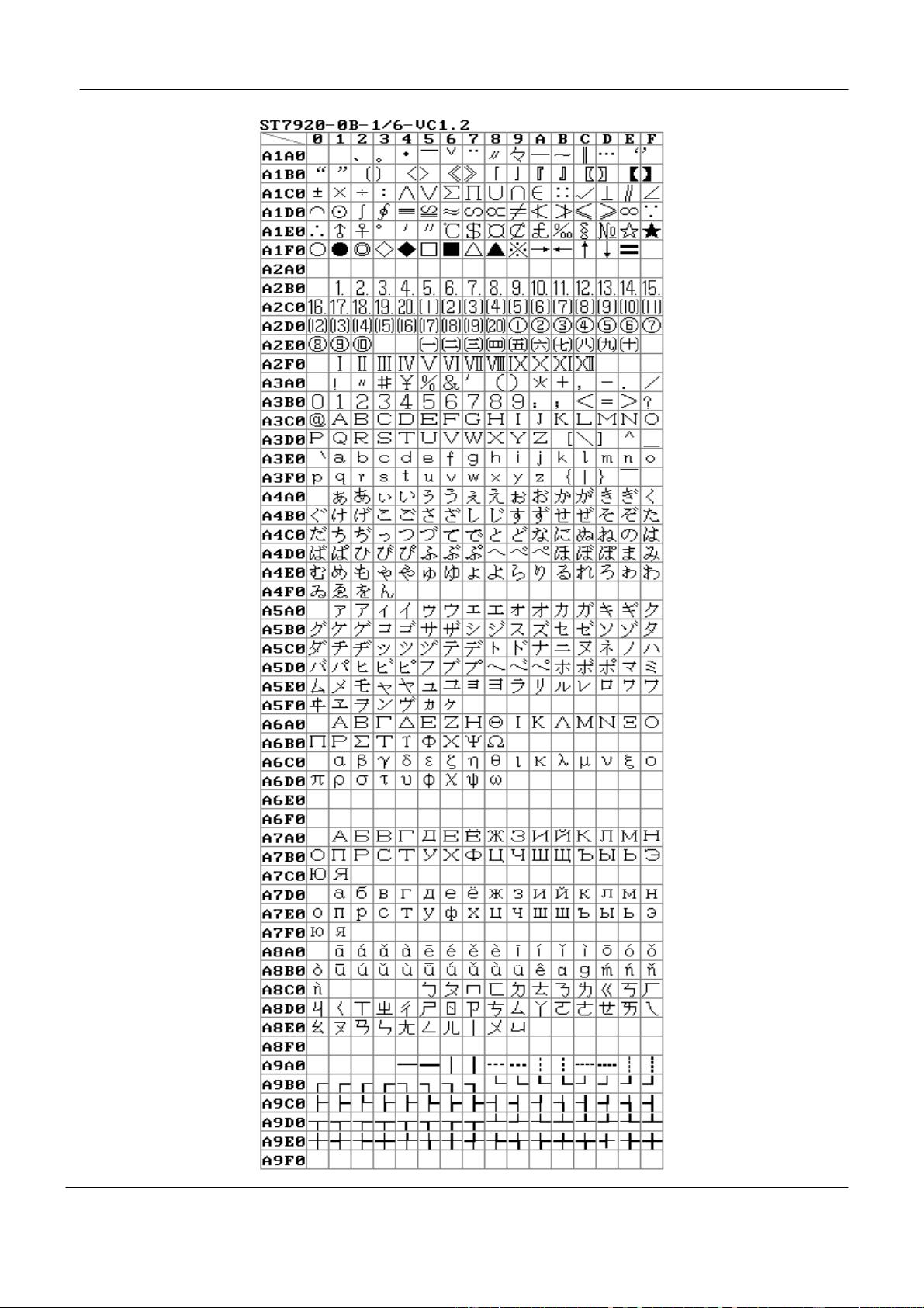
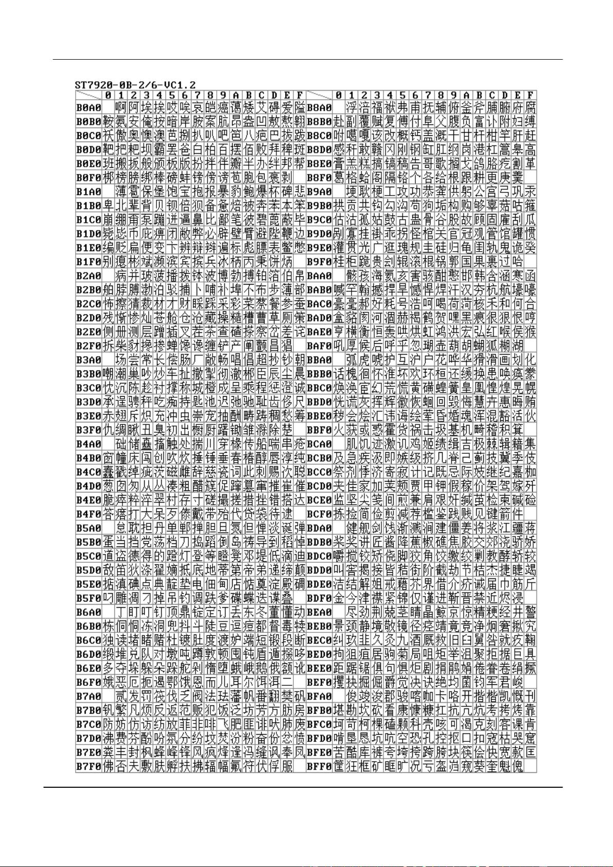
.Control IC: ST7920 ST7921
.Background color: Yellow (White)
.Glass to PCB: ZEBRA CONNECTO
.Operating temperature:-20~70°C
.Storage temperature:-30~80°C
. Dot Size : 0.48x 0.48 mm
. Dot Pitch : 0.52 x 0.52 mm
2.0 MAX STANDARD VALUE
ITEM SYMBOL MIN TYPE MAX UNIT
OPERATING TEMPERATURE Top -20 25 70
℃
STORAGE TEMPERATURE Tst -30 25 80
℃
SUPPLY VOLTAGE FOR LOGIC VDD-VSS 2.7 5.0 5.5 V
3.0 ELECTRICAL CHARACTERISTICS
ITEM SYMBOL CONDITION MIN. TYP. MAX. UNIT
SUPPLY VOLTAGE FOR
LOGIC
V
DD
-V
SS
Ta = 25
°
C
4.5 5.0 5.5 V
INPUT HIGH VOL.
V
IH
Ta = 25
°
C
V
DD-1
- V
DD
V
INPUT LOW VOL.
V
IL
Ta = 25
°
C
V
SS
- 1.0 V
OUTPUT HIGH VOL.
V
OH
Ta = 25
°
C
0.8V
DD
- V
DD
V
OUTPUT LOW VOL.
V
OL
Ta = 25
°
C
- - 0.1V
DD
V
4.0 MECHANICAL SPECIFICATIONS
ITEM STANDARD VALUE UNIT
PCB Dimension 93.0X70.0X1.60 mm
View Dimension
73.0X39.0 mm
Outline Dimension 93.0X70.0X13.0 mm
YJD12864C-1 LCD Module Specification Ver1.0
电
电
话
话
:
:
0
0
7
7
5
5
5
5
-
-
2
2
7
7
6
6
6
6
8
8
0
0
3
3
0
0 27668083 传 真:
0
0
7
7
5
5
5
5
-
-
2
2
7
7
6
6
6
6
8
8
0
0
3
3
0
0
-
-
6
6
0
0
6
6
地址:深圳市宝安 32 区裕安二路 208 号
3
5.0 EXTERNAL DIMENSIONS
5.1 SYSTEM BLOCK DIAGRAM
YJD12864C-1 LCD Module Specification Ver1.0
电
电
话
话
:
:
0
0
7
7
5
5
5
5
-
-
2
2
7
7
6
6
6
6
8
8
0
0
3
3
0
0 27668083 传 真:
0
0
7
7
5
5
5
5
-
-
2
2
7
7
6
6
6
6
8
8
0
0
3
3
0
0
-
-
6
6
0
0
6
6
地址:深圳市宝安 32 区裕安二路 208 号
4
6.0 INTERFACE PIN FUNCTION DESCRIPTION
PIN NO
SYMBOL
FUNCTION
1
VSS
Ground(0V)
2
VDD
Power supply for logic circuit(5.0V)
3
VO
Operating voltage for LCD driving(Not connected)
4
D/I(CS*)
Register select
0: select instruction write, busy flag read, address
counter read
1: select data write, read
(Chip select) for serial mode
1: chip enable 0: chip disable
5
R/W(SID*)
Read write control
0: write 1: read
(serial data input)
6
E(SCLK*)
Enable trigger (serial clock)
7-10 DB0 to DB3
Lower nibble data bus for 8 bit interface
11-14 DB4 to DB7
Higher nibble data bus for 8 bit interface and
data bus for 4 bit interface
15
PSB
Interface selection:
0: serial mode 1: 8/4-bits parallel bus mode
16
NC
Not connected
17
RSTB
System reset low active
18
VEE
Not connected
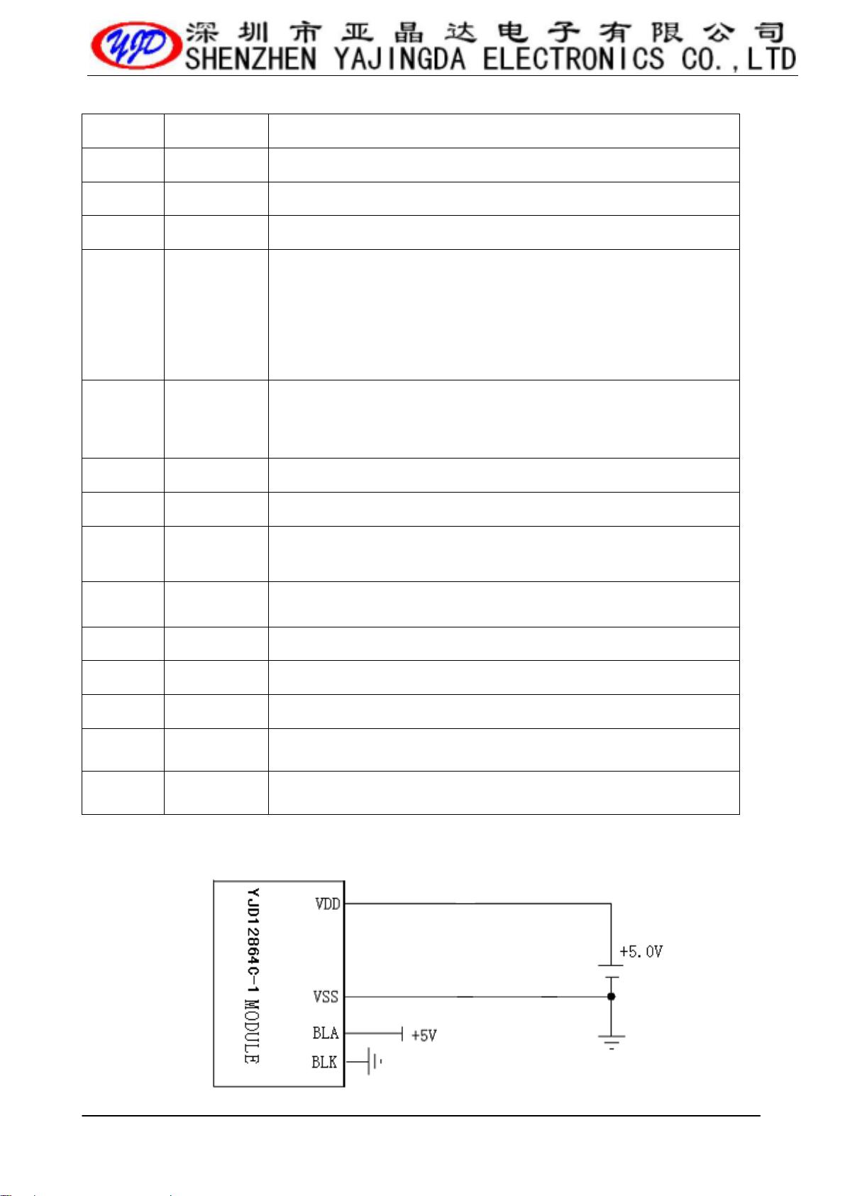
19
BLA
Backlight (+5.0V)
20
BLK
Backlight (0V)
7.0 POWER SUPPLY BLOCK DIAGRAM
YJD12864C-1 LCD Module Specification Ver1.0
电
电
话
话
:
:
0
0
7
7
5
5
5
5
-
-
2
2
7
7
6
6
6
6
8
8
0
0
3
3
0
0 27668083 传 真:
0
0
7
7
5
5
5
5
-
-
2
2
7
7
6
6
6
6
8
8
0
0
3
3
0
0
-
-
6
6
0
0
6
6
地址:深圳市宝安 32 区裕安二路 208 号
5
8.0 TIMING CHARACTERISTICS
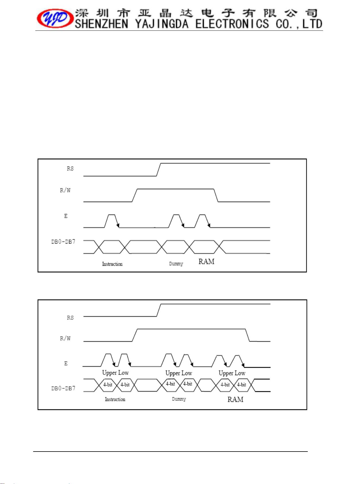
Parallel interface :
YJD12864C-1 is in parallel mode by pulling up PSB pin. And can select 8 bit or 4-bit
bus interface by function set instruction DL control bit. MPU can control ( RS , RW ,
E , and DB0..DB7 ) pins to complete the data transmission.
In 4-bit transfer mode, every 8 bits data or instruction is separated into 2 parts.
Higher 4 bits(DB7~DB4)data will transfer
First and placed into data pins(DB7~DB4). Lower 4 bits(DB3~DB0)data will transfer
second and placed into data pins (DB7~DB4). (DB3~DB0) data pins are not used.
Timing Diagram of 8-bit Parallel Bus Mode Data Transfer
Timing Diagram of 4-bit Parallel Bus Mode Data Transfer


