没有合适的资源?快使用搜索试试~ 我知道了~
资源推荐
资源详情
资源评论
![rar](https://img-home.csdnimg.cn/images/20210720083606.png)
![zip](https://img-home.csdnimg.cn/images/20210720083736.png)
![7z](https://img-home.csdnimg.cn/images/20210720083312.png)
![zip](https://img-home.csdnimg.cn/images/20210720083736.png)
![rar](https://img-home.csdnimg.cn/images/20210720083606.png)
![](https://csdnimg.cn/release/download_crawler_static/87512908/bg1.jpg)
www.3peakic.com.cn
Rev.A.6
1 / 22
TPAFE0808
8-Channel Configurable ADC/DAC with I
2
C interface
Features
8-channel, configurable ADC/DAC/GPIO
8 12-bit DAC channels
8 12-bit ADC channels
8 general-purpose I/O pins
Integrated temperature sensor
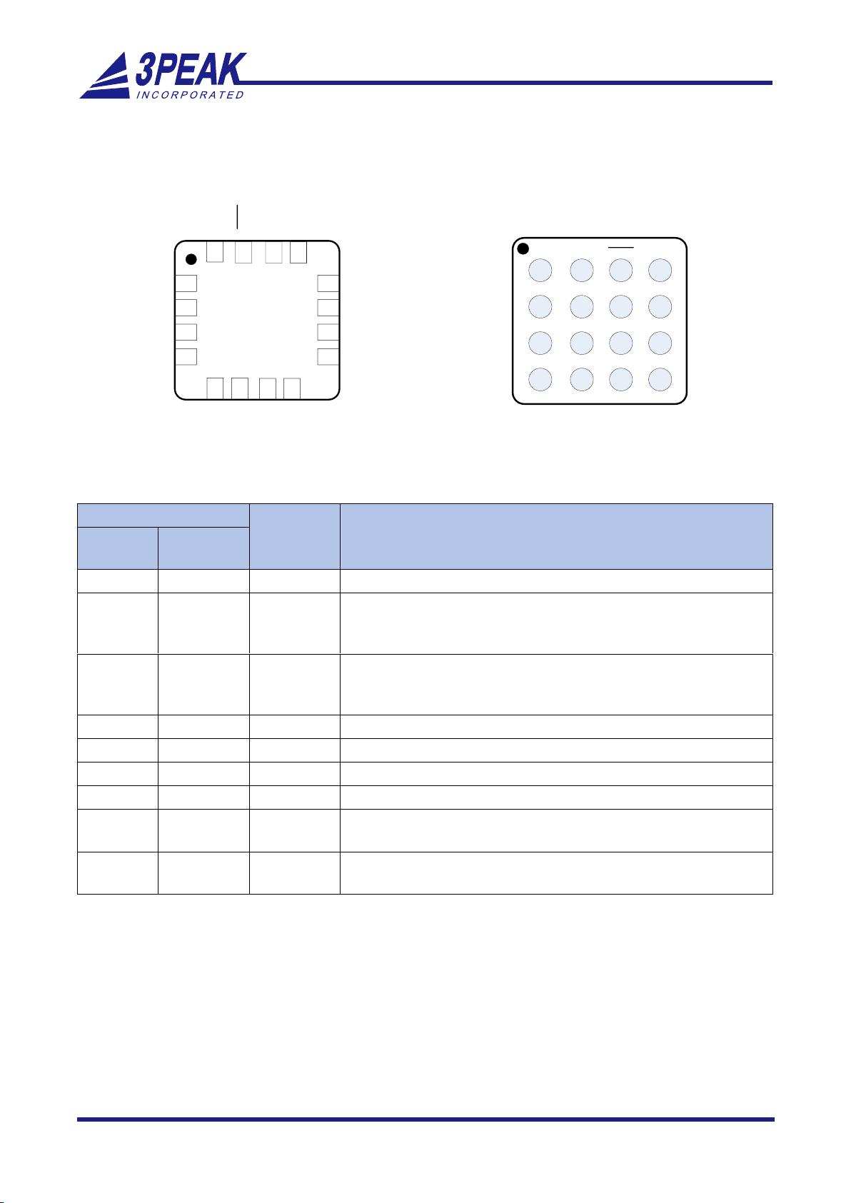
16-lead MIS 3x3 and 16-ball WLCSP 2x2 package
I
2
C interface
Applications
General-purpose analog and digital I/O
Multi channels Control and monitor
Description
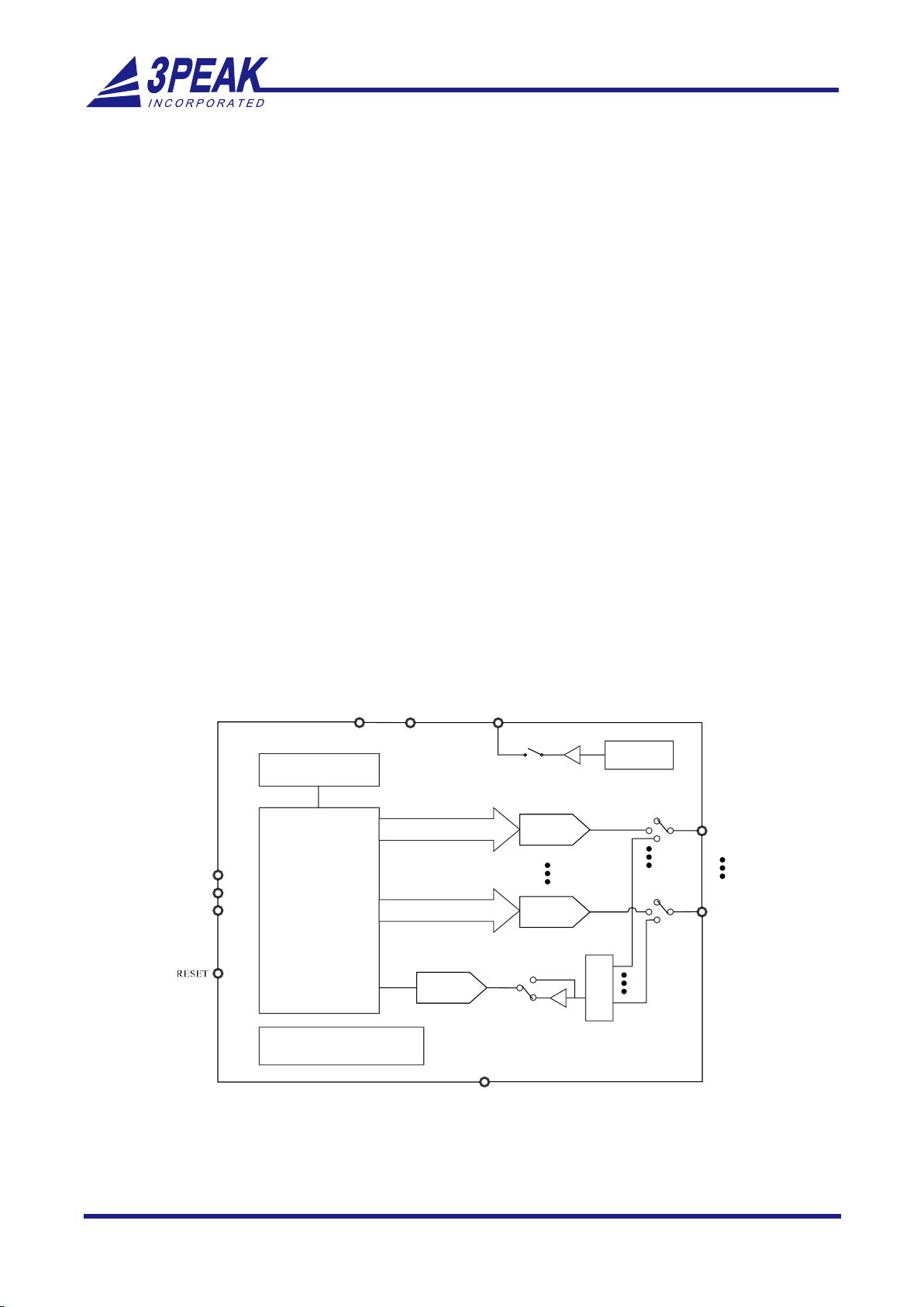
The TPAFE0808 has eight input/output pins, which
can be configured to be ADC input, or DAC output, or
General purpose I/O pins.
A 12bit ADC is integrated in TPAFE0808, which can
be connected to each input/output pin by an eight-
channel multiplexer. The ADC input range is 0~VREF
or 0~2*VREF.
TPAFE0808 has eight channel 12bit DAC, which can
be connected to corresponding input/output pin. The
DAC output range is 0~VREF or 0~2*VREF.
TPAFE0808 has an internal 2.5V reference, and it
can also use external reference when internal
reference is turned off.
It also has an internal temperature sensor which can
measure die temperature.
The TPAFE0808 is available in 16-lead MIS 3x3, as
well as a 16-ball WLCSP, and operates over a
temperature range of −40°C to +125°C.
Function Block Diagram
![](https://csdnimg.cn/release/download_crawler_static/87512908/bg2.jpg)
www.3peakic.com.cn
Rev.A.6
2 / 22
TPAFE0808
8-Channel Configurable ADC/DAC with I
2
C interface
Table of Contents
Features .............................................................................................................................................................. 1
Applications ....................................................................................................................................................... 1
Description ......................................................................................................................................................... 1
Function Block Diagram ................................................................................................................................... 1
Revision History ................................................................................................................................................ 3
Pin Configuration and Functions ..................................................................................................................... 4
Pin Functions ................................................................................................................................................ 4
Specifications .................................................................................................................................................... 5
Absolute Maximum Ratings
(1)
....................................................................................................................... 5
ESD, Electrostatic Discharge Protection ...................................................................................................... 5
Thermal Information ..................................................................................................................................... 5
Electrical Characteristics .............................................................................................................................. 6
Typical Performance Characteristics ............................................................................................................ 9
Detail Description ............................................................................................................................................ 10
Register Map .............................................................................................................................................. 10
Register Explanations ................................................................................................................................ 10
Feature Description .................................................................................................................................... 15
Application Information .................................................................................................................................. 19
Tape and Reel Information .............................................................................................................................. 20
Package Outline Dimensions ......................................................................................................................... 21
MIS3X3-16L ................................................................................................................................................ 21
WLCSP 2x2-16L ......................................................................................................................................... 22
Order Information ............................................................................................................................................ 22
![](https://csdnimg.cn/release/download_crawler_static/87512908/bg3.jpg)
www.3peakic.com.cn
Rev.A.6
3 / 22
TPAFE0808
8-Channel Configurable ADC/DAC with I
2
C interface
Revision History
Date
Revision
Notes
2020/8/2
Rev.A.1
1.0 Version
2020/9/11
Rev.A.2
Refine parameters, and update register definition details
2021/1/19
Rev.A.3
Update serial interface diagram
2021/5/20
Rev.A.4
Update Product description and diagram.
2021/7/22
Rev.A.5
Update t3 tLOW Max limit
2022/7/28
Rev.A.6
Update tape and reel information
![](https://csdnimg.cn/release/download_crawler_static/87512908/bg4.jpg)
www.3peakic.com.cn
Rev.A.6
4 / 22
TPAFE0808
8-Channel Configurable ADC/DAC with I
2
C interface
Pin Configuration and Functions
MIS3X3-16L Configuration
WLCSP 2x2-16L (Top View, Ball side down)
Pin Functions
Pin No.
Pin Name
Description
MIS3X3-
16L
WLCSP 2x2-
16L
1
B4
VDD
Power Supply Input.
2 to 5,
8 to 11
B3, C4, C3,
C2, D1, D4,
C1, B2
I/O0 to I/O7
Input/Output pin. These pins can be configured as DACs, ADCs, or GPIO
independently.
6
D3
VREF
Reference Input/Output. When the internal reference is enabled, the 2.5 V
voltage is available on the pin. When the internal reference is disabled,
an external reference should be used and connected to the pin.
7
D2
VLOGIC
Digital interface Power Supply.
12
B1
GND
Ground.
13
A1
SDA
Serial Data Line. This pin is open drain input/output.
14
A2
SCL
Serial Clock Line. This pin is open drain input.
15
A3
/RESET
Reset Pin. Low effective. When this pin is tied low, the chip is reset to
default condition.
16
A4
A0
Address pin. It can be connected to GND or VLOGIC. It sets LSB of I
2
C
address.
2
1
A
B
C
D
3
4
SDA SCL RESET
A0
GND I/O7
I/O0 VDD
I/O6 I/O3
I/O2 I/O1
I/O4 VLOGIC
VREF I/O5
15
16
1
2
3
4
5
6
14
13
12
11
10
9
8
7
TPAFE0808
TOP VIEW
RESET
A0
VDD
I/O0
I/O1
I/O2
I/O3
VREF
SCL
SDA
GND
I/O7
I/O6
I/O5
I/O4
VLOGIC
![](https://csdnimg.cn/release/download_crawler_static/87512908/bg5.jpg)
www.3peakic.com.cn
Rev.A.6
5 / 22
TPAFE0808
8-Channel Configurable ADC/DAC with I
2
C interface
Specifications
Absolute Maximum Ratings
(1)
Parameter
Rating
VDD to GND
−0.3 V to +7 V
VLOGIC to GND
−0.3 V to +7 V
Analog Input Voltage to GND
−0.3 V to VDD + 0.3 V
Digital Input Voltage to GND
−0.3 V to VLOGIC + 0.3 V
Digital Output Voltage to GND
−0.3 V to VLOGIC +0.3 V
VREF to GND
−0.3 V to VDD +0.3 V
Operating Temperature Range
−40°C to +125°C
Storage Temperature Range
−65°C to +150°C
Junction Temperature (T
J
max)
+150°C
Note (1): Stresses beyond those listed under Absolute Maximum Ratings may cause permanent damage to the device.
Exposure to Absolute Maximum Rating conditions for extended periods may affect device reliability.
ESD, Electrostatic Discharge Protection
Symbol
Parameter
Condition
Minimum Level
Unit
HBM
Human Body Model ESD
ANSI/ESDA/JEDEC JS-001
6
kV
CDM
Charged Device Model ESD
ANSI/ESDA/JEDEC JS-002
1.5
kV
Thermal Information
Package Type
θ
JA
θ
JC
Unit
MIS3X3-16L
100.1
37.4
°C/W
WLCSP 2x2-16L
70
28.6
°C/W
剩余21页未读,继续阅读
资源评论
![avatar-default](https://csdnimg.cn/release/downloadcmsfe/public/img/lazyLogo2.1882d7f4.png)
![avatar](https://profile-avatar.csdnimg.cn/default.jpg!1)
Wums305623673
- 粉丝: 0
- 资源: 3
上传资源 快速赚钱
我的内容管理 展开
我的资源 快来上传第一个资源
我的收益
登录查看自己的收益我的积分 登录查看自己的积分
我的C币 登录后查看C币余额
我的收藏
我的下载
下载帮助
![voice](https://csdnimg.cn/release/downloadcmsfe/public/img/voice.245cc511.png)
![center-task](https://csdnimg.cn/release/downloadcmsfe/public/img/center-task.c2eda91a.png)
最新资源
- AutoHotKey 2.0中文帮助文件
- 基于Docker-compose的Elasticsearch集群每个节点均是独立docker-compose配置而成源码.zip
- 目标检测-零售食品LOGO检测数据集-40000张图-+对应VOC-COCO-YOLO三种格式标签+数据集划分脚本
- 目标检测-零售食品LOGO检测数据集-30000张图-+对应VOC-COCO-YOLO三种格式标签+数据集划分脚本
- 目标检测-零售食品LOGO检测数据集-20000张图-+对应VOC-COCO-YOLO三种格式标签+数据集划分脚本
- 目标检测-零售食品LOGO检测数据集-10000张图-+对应VOC-COCO-YOLO三种格式标签+数据集划分脚本
- 基于GUI+MYSQL+JAVA图书管理系统文档说明+源码(高分大作业项目).zip
- 基于Qt使用C++实现图书管理系统源码+数据库(95分以上).zip
- 基于GUI+MYSQL+JAVA票务管理系统文档介绍+源码+数据库(高分大作业).zip
- Java项目-购物网站系统(java+Servlet+JSP+Mysql)
资源上传下载、课程学习等过程中有任何疑问或建议,欢迎提出宝贵意见哦~我们会及时处理!
点击此处反馈
![feedback](https://img-home.csdnimg.cn/images/20220527035711.png)
![feedback-tip](https://img-home.csdnimg.cn/images/20220527035111.png)
安全验证
文档复制为VIP权益,开通VIP直接复制
![dialog-icon](https://csdnimg.cn/release/downloadcmsfe/public/img/green-success.6a4acb44.png)