Control of radiation angle by
introducing symmetric end structure to
oblique waveguide in three-dimensional
photonic crystal
Kou Gondaira,
∗
Kenji Ishizaki, Keisuke Kitano, Takashi Asano, and
Susumu Noda
Department of Electronic Science and Engineering, Kyoto University, Kyoto 615-8510, Japan
∗
kou.gondaira@qoe.kuee.kyoto-u.ac.jp
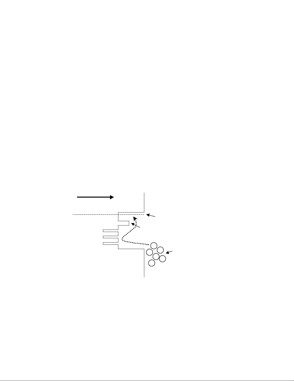
Abstract: We investigate the radiation angle of an oblique waveguide
in a stripe-stacked three-dimensional photonic crystal. We show that the
output-light is radiated in a different direction from the oblique waveguide
direction. Moreover, the radiation polar angle varies from 30
◦
to 50
◦
depending on the frequency. To inhibit the frequency dependence and
obtain vertical radiation, we introduced a symmetric structure at the end
of the waveguide. As a result of cancellation of the in-plane asymmetric
wavenumber, the radiation polar angle is less than 6
◦
from the surface-
normal direction and does not depend on frequency.
© 2016 Optical Society of America
OCIS codes: (230.7370) Waveguides; (160.5298) Photonic crystals; (130.5296) Photonic crys-
tal waveguides.
References and links
1. E. Yablonovitch, “Inhibited spontaneous emission in solid-state physics and elecronics,” Phys. Rev. Lett. 58(20),
2059–2062 (1987).
2. S. Noda, K. Tomoda, N. Yamamoto, and A. Chutinan, “Full three-dimensional photonic bandgap crystals at
near-infrared wavelengths,” Science 289, 604–606 (2000).
3. K. Aoki, H. T. Miyazaki, H. Hirayama, K. Inoshita, T. Baba, K. Sakoda, N. Shinya, and Y. Aoyagi, “Microassem-
bly of semiconductor three-dimensional photonic crystals,” Nat. Mater. 2, 117–121 (2003).
4. M. Qi, E. Lidorikis, P. T. Rakich, S. G. Johnson, J. Joannopoulos, E. P. Ippen, and H. I. Smith, “A three-
dimensional optical photonic crystal with designed point defects,” Nature 429, 538–542 (2004).
5. S. Ogawa, M. Imada, S. Yoshimoto, M. Okano, and S. Noda, “Control of light emission by 3D photonic crystals,”
Science 305, 227–229 (2004).
6. M. Maldovan and E. L. Thomas, “Diamond-structured photonic crystals,” Nat. Mater. 3, 593–600 (2004).
7. S. Takahashi, K. Suzuki, M. Okano, M. Imada, T. Nakamori, Y. Ota, K. Ishizaki, and S. Noda, “Direct creation
of three-dimensional photonic crystals by a top-down approach,” Nat. Mater. 8, 721–725 (2009).
8. I. Staude, M. Thiel, S. Essig, C. Wolff, K. Busch, G. von Freymann, and M. Wegener, “Fabrication and char-
acterization of silicon woodpile photonic crystals with a complete bandgap at telecom wavelengths,” Opt. Lett.
35(7), 1094–1096 (2010).
9. I. Staude, G. von Freymann, S. Essig, K. Busch, and M. Wegener, “Waveguides in three-dimensional photonic-
bandgap materials by direct laser writing and silicon double inversion,” Opt. Lett. 36(1), 67–69 (2011).
10. W. J. Chen, Z. H. Hang, J. W. Dong, X. Xiao, H. Z. Wang, and C. T. Chan, “Observation of backscattering-
immune chiral electromagnetic modes without time reversal breaking,” Phys. Rev. Lett. 107, 023901 (2011).
11. I. Staude, C. McGuinness, A. Frlich, R. L. Byer, E. Colby, and M. Wegener, “Waveguides in three-dimensional
photonic bandgap materials for particle-accelerator on a chip architectures,” Opt. Express 20, 5607–5612 (2012).
12. K. Suzuki, K. Kitano, K. Ishizaki, and S. Noda, “Three-dimensional photonic crystals created by single-step
multi-directional plasma etching,” Opt. Express 22, 17099–17106 (2014).
#260943
Received 10 Mar 2016; revised 26 May 2016; accepted 27 May 2016; published 9 Jun 2016
(C) 2016 OSA
13 Jun 2016 | Vol. 24, No. 12 | DOI:10.1364/OE.24.013518 | OPTICS EXPRESS 13518