


BK3435 Datasheet V 2.8
© 2017 Beken Corporation Proprietary and Confidential Page 1 of 21
BK3435 Bluetooth Low Energy
Single Mode SoC
Beken Corporation
Building 41, Capital of Tech Leaders, 1387 Zhangdong Road,
Zhangjiang High-Tech Park, Pudong New District, Shanghai, China
Tel: (86)21 51086811
Fax: (86)21 60871089
This document contains information that may be proprietary to, and/or secrets of, Beken Corporation. The
contents of this document should not be disclosed outside the companies without specific written permission.
Disclaimer: Descriptions of specific implementations are for illustrative purpose only, actual hardware
implementation may differ.

BK3435 Datasheet V 2.8
© 2017 Beken Corporation Proprietary and Confidential Page 2 of 21
Table of Contents
1 General Description ........................................................................................... 3
1.1 Overview ..................................................................................................... 3
1.2 Block Diagram ............................................................................................. 3
1.3 Features ...................................................................................................... 4
2 PIN information .................................................................................................. 5
2.1 QFN32 ......................................................................................................... 5
2.2 QFN40 ......................................................................................................... 6
2.3 QFN48(BK3435QN48A) .............................................................................. 8
2.4 QFN48(BK3435QN48B) ............................................................................ 10
3 Functional Description ..................................................................................... 11
3.1 GPIO ......................................................................................................... 11
3.2 Timers ....................................................................................................... 13
3.2.1 PWM Timers ....................................................................................... 13
3.2.2 3DS Timers ......................................................................................... 13
3.2.3 Watch dog timer and RTC timer ......................................................... 13
3.3 ADC ........................................................................................................... 13
3.4 UART, I2C and SPI ................................................................................... 14
3.5 Audio interface .......................................................................................... 14
3.6 IrDA Transceiver ....................................................................................... 14
3.7 USB ........................................................................................................... 15
3.8 True random number generator ................................................................ 15
3.9 I2S Digital Audio ........................................................................................ 15
4 Electrical Specifications ................................................................................... 15
5 Package Information ........................................................................................ 18
5.1 QFN 4x4 32-Pin ......................................................................................... 18
5.2 QFN 5x5 40-Pin ......................................................................................... 19
5.3 QFN 6x6 48-Pin ......................................................................................... 20
6 Order Information ............................................................................................. 21

BK3435 Datasheet V 2.8
© 2017 Beken Corporation Proprietary and Confidential Page 3 of 21
1 General Description
1.1 Overview
The BK3435 chip is a highly integrated Bluetooth low energy single mode device
certified with BLE 5.0 (DID: D040065). It integrates a high-performance RF
transceiver, baseband, MCU core, rich feature peripheral units, programmable
protocol and profile to support BLE application. The Flash program memory
makes it suitable for customized applications.
The BK3435 is designed with advanced technology process and integrated with
switch DCDC regulator, that it has ultra-low power consumption and ultra-low
leakage power. The embedded high order interference suppression filter and fast
automatic gain control logic make it work well in high interference environment.
1.2 Block Diagram
ARM968E-S
Data Memory
(64 KB)
Program Memory
(500 KB FLASH)
PWMs
SPI
I2C
2 UARTs
ADCs
IrDA Amp.
USB
Microphone
RF TRX
RTC Timer
Temperature
Sensor
Power
Managerment
32 kHz
ROSC
Bluetooth LE
4.2
I2S/PCM
True Random
Number Generator
Watch Dog
10 Times
I2S Master
Clock PLL
64 MHz
DPLL
16 MHz
32 kHz
Crystal
Figure 1 BK3435 Block Diagram

BK3435 Datasheet V 2.8
© 2017 Beken Corporation Proprietary and Confidential Page 4 of 21
1.3 Features
BLE with 1 Mbps and 2 Mbps rate and extended data length
Enhanced privacy with BLE 4.2 secure connection
Support BLE master and slave links at the same time
Low-power 2.4 GHz Transceiver
32-bit RISC Core integrated
500 KB programmable Flash for Program and 64 KB RAM for Data
Operation voltage from 0.9 V to 3.6 V
Clock
16 MHz crystal reference clock with internal tuning load capacitance
64 MHz digital PLL clock
32 kHz ring oscillator
External 32KHz crystal oscillator
MCU can run with any clock source with internal frequency divider
Dedicate audio PLL clock for I2S main clock
Interface and peripheral units
Quad IO FLASH programming
JTAG, I2C, SPI interface
Two UART interface
Multi-channels PWM output
USB Host and Device interface
IrDA receiver and transmitter amplify
On-chip high accurate temperature sensor
On-chip 10 bit general ADC
On-chip audio gain amplify and 16 bit microphone ADC
GPIO with multiplexed interface functions
True random number generator
I2S/PCM digital audio interface with master and slave mode
Typical Package Type
32-pin QFN 4x4, 40-pin QFN5x5 and 48-pin QFN6x6
BK3435 Datasheet V 2.8
© 2017 Beken Corporation Proprietary and Confidential Page 5 of 21
2 PIN information
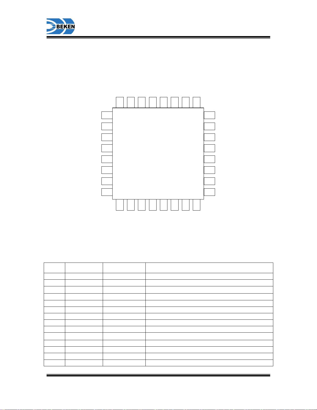
2.1 QFN32
9
1
0
1
1
1
2
1
3
1
4
1
5
1
6
P
05
VCCRF
P
03
P
07
P
02
1
2
3
4
5
6
7
8
24
23
22
21
20
19
18
17
3
2
3
1
3
0
2
9
2
8
2
7
2
6
2
5
BK3435
4x4 QFN32
P
04
P
06
ANT
VCCIF
XTALO
XTALI
P31
P32
XTAL32K
SW
VCCBAT
CP
1
CP
2
VCPOUT
VCCMCU
P
00
P
01
P10
P11
RSTN
VDDSPI
VBAT1V
VSSBAT
MIC_BIAS
MICN
MICP
P33
Figure 2 BK3435 QFN32 pin assignment
Table 1 BK3435 QFN32 Pin Description
PIN
Name
Pin Function
Description
1
VCCIF
Power
IF power, 1.5 V
2
XTALO
Analog
16 MHz crystal output
3
XTALI
Analog
16 MHz crystal input
4
P31
Digital I/O
General purpose IO
5
P32
Digital I/O
General purpose IO
6
P10
Digital I/O
General purpose IO
7
P11
Digital I/O
General purpose IO
8
RSTN
Analog
Active low pin reset
9
XTAL32K
Analog
32 kHz Crystal input
10
MIC_BIAS
Analog
Microphone bias voltage output, 1.5 V
11
MIC_N
Analog
Microphone input N
12
MIC_P
Analog
Microphone input P
13
P33
Digital I/O
General purpose IO
14
VDDSPI
Analog
LDO output, 1.5 V


