ON-N64S830HA.PDF
需积分: 9 116 浏览量
2021-04-28
21:07:41
上传
评论
收藏 149KB PDF 举报

© Semiconductor Components Industries, LLC, 2012
June, 2012 − Rev. 12
1 Publication Order Number:
N64S830HA/D
N64S830HA
64 kb Low Power Serial
SRAMs
8 k x 8 Bit Organization
Introduction
The ON Semiconductor serial SRAM family includes several
integrated memory devices including this 64 k serially accessed Static
Random Access Memory, internally organized as 8 k words by 8 bits.
The devices are designed and fabricated using ON Semiconductor’s
advanced CMOS technology to provide both high−speed performance
and low power. The devices operate with a single chip select (CS
)
input and use a simple Serial Peripheral Interface (SPI) serial bus. A
single data in and data out line is used along with a clock to access data
within the devices. The N64S830HA devices include a HOLD
pin that
allows communication to the device to be paused. While paused, input
transitions will be ignored. The devices can operate over a wide
temperature range of −40°C to +85°C and can be available in several
standard package offerings.
Features
• Power Supply Range: 2.5 to 3.6 V
• Very Low Standby Current: As low as 1 mA
• Very Low Operating Current: As low as 3 mA
• Simple Memory Control:
Single chip select (CS
)
Serial input (SI) and serial output (SO)
• Flexible Operating Modes:
Word read and write
Page mode (32 word page)
Burst mode (full array)
• Organization: 8 k x 8 bit
• Self Timed Write Cycles
• Built−in Write Protection (CS High)
• HOLD Pin for Pausing Communication
• High Reliability: Unlimited write cycles
• Green SOIC and TSSOP
• These Devices are Pb−Free, Halogen Free/BFR Free and are RoHS
Compliant
http://onsemi.com
Device Package
ORDERING INFORMATION
N64S830HAS22I SOIC−8
(Pb−Free)
Shipping
†
100 Units / Tube
N64S830HAT22I TSSOP−8
(Pb−Free)
100 Units / Tube
N64S830HAS22IT SOIC−8
(Pb−Free)
3000 / Tape &
Reel
N64S830HAT22IT TSSOP−8
(Pb−Free)
3000 / Tape &
Reel
†For information on tape and reel specifications,
including part orientation and tape sizes, please
refer to our Tape and Reel Packaging Specification
Brochure, BRD8011/D.
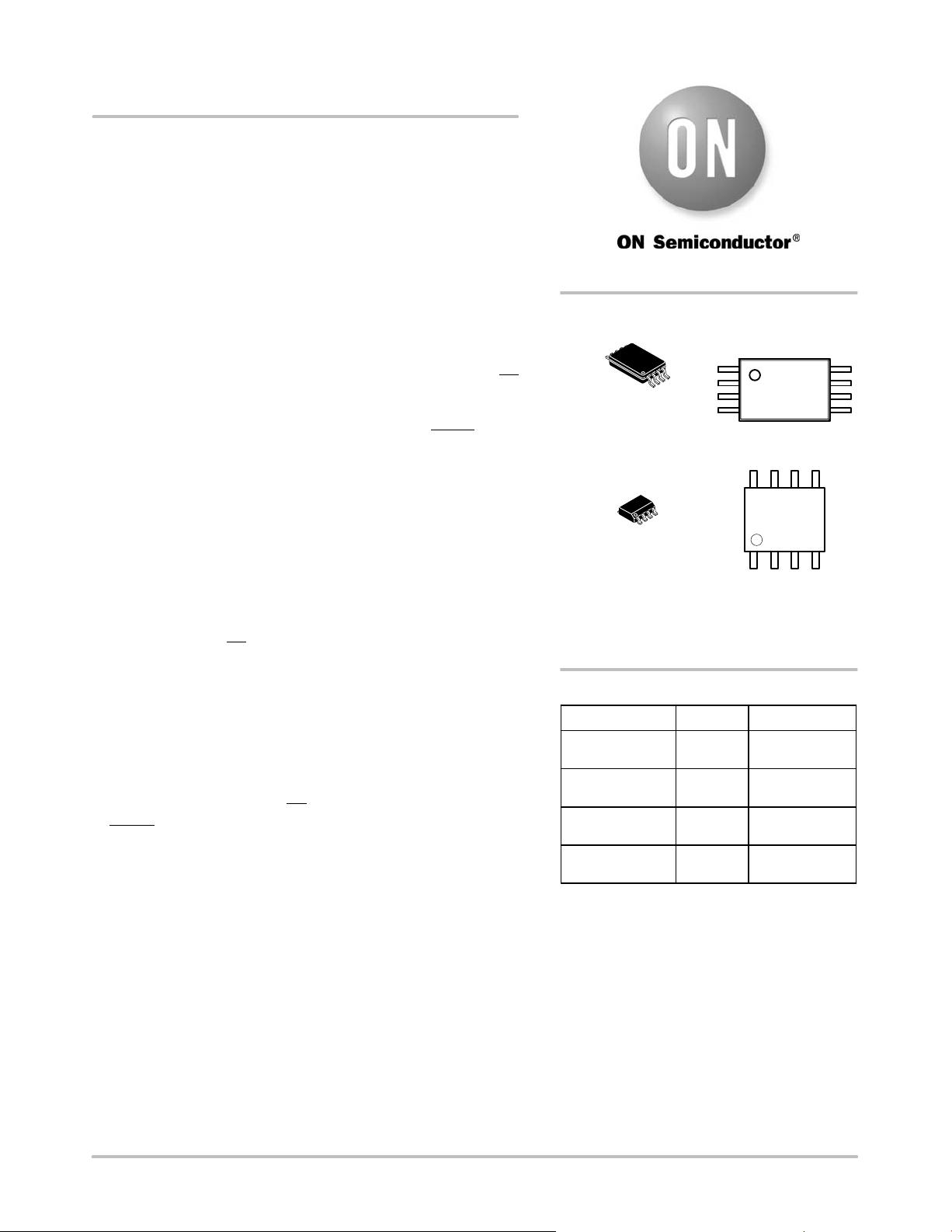
TSSOP−8
T SUFFIX
CASE 948AL
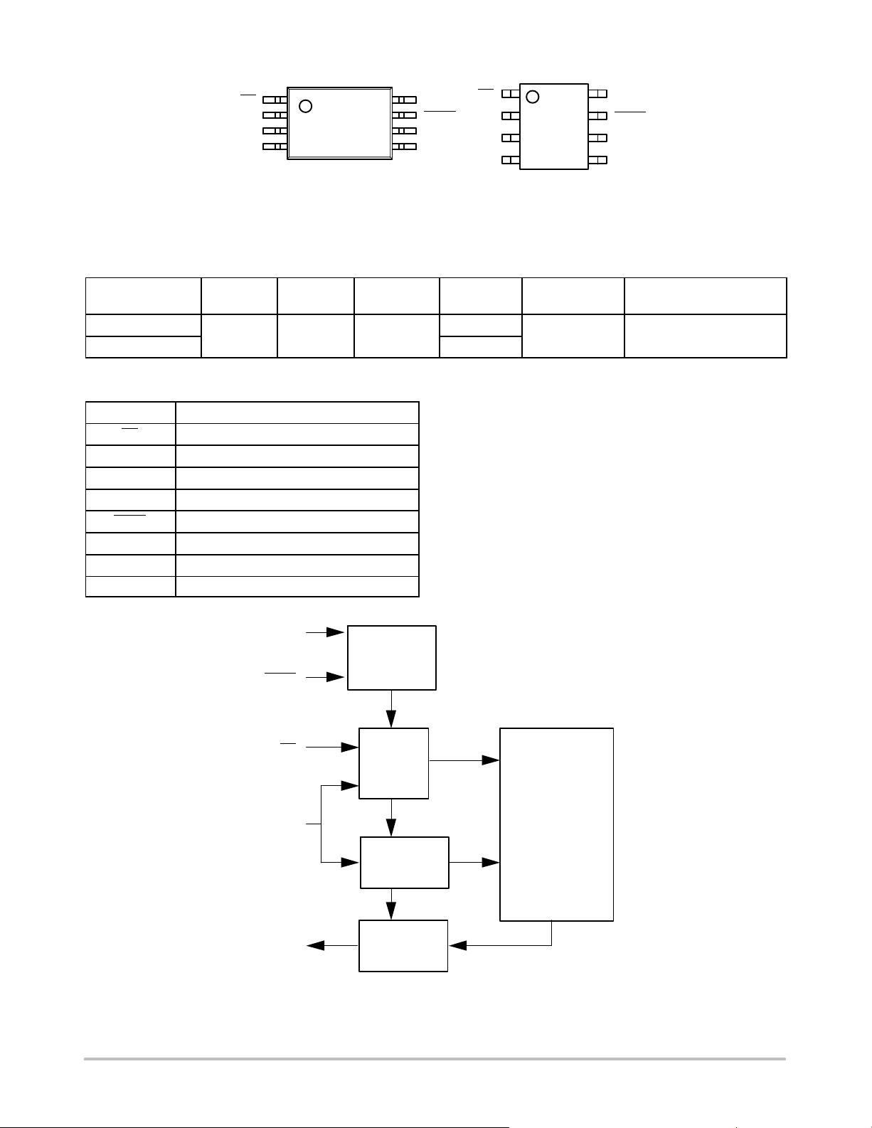
MARKING
DIAGRAMS
B125
XXXXYZZ
XXXX = Date Code
Y = Assembly Code
ZZ = Lot Traceability
SOIC−8
S SUFFIX
CASE 751BD
B115
XXXXYZZ
剩余12页未读,继续阅读
资源评论


