

5
5
4
4
3
3
2
2
1
1
D D
C C
B B
A A
Drawing Title:
Size Document Number Rev
Date: Sheet
of
Page Title:
Designer:
Drawn by:
Approved:
Multimedia Application Division,
Wireless & Mobile System Group
This document contains information proprietary to Freescale Semiconductor and shall not be used for
engineering design, procurement or manufacture in whole or in part without the express written permission
of Freescale Semiconductor.
SOURCE:SCH-xxxxx PDF:SPF-xxxxx 0.1
MX6Q TurnKey
C
Wednesday, January 16, 2013
Cover
<Designer>
<Approver>
<DrawnBy>
123
1
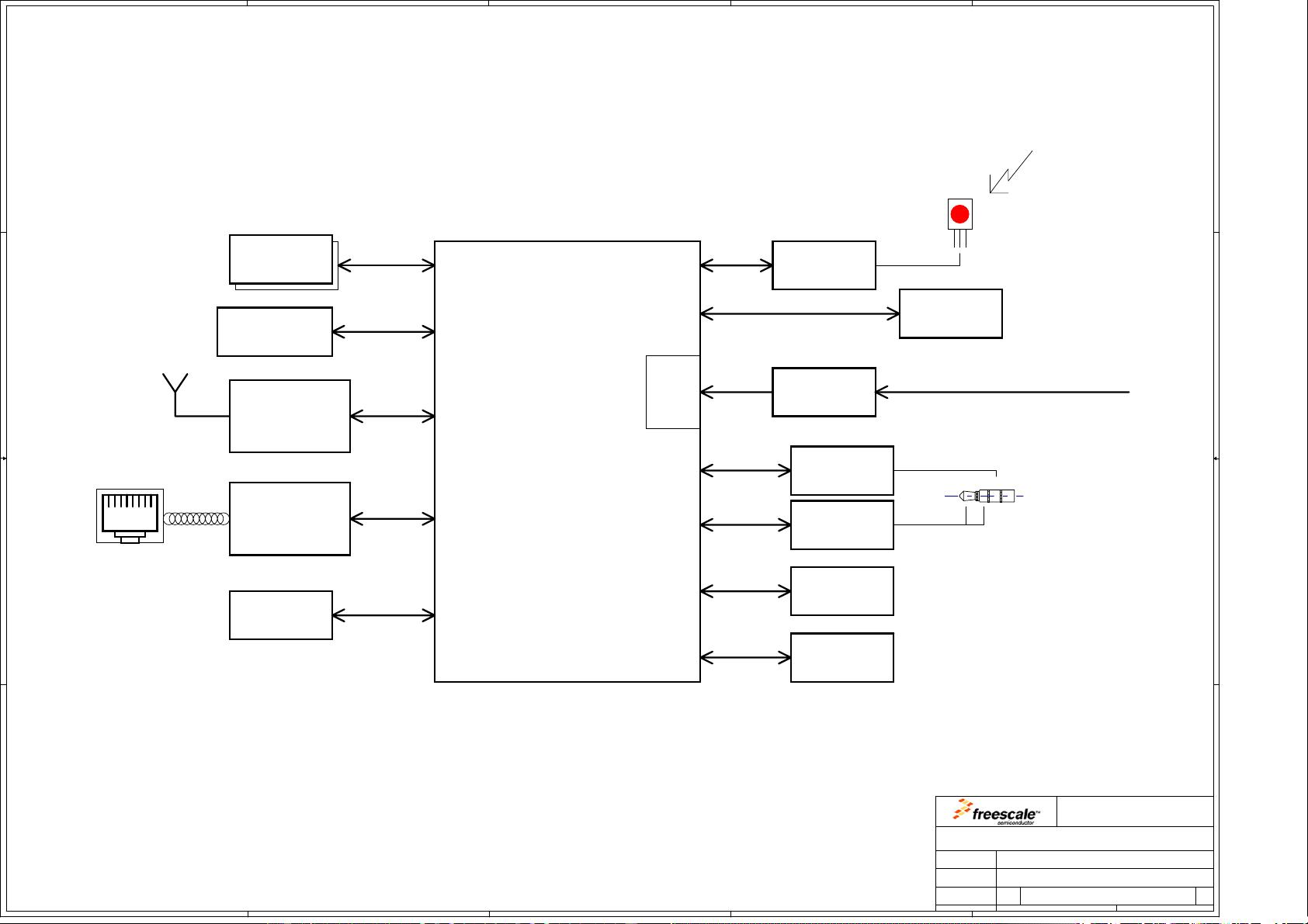
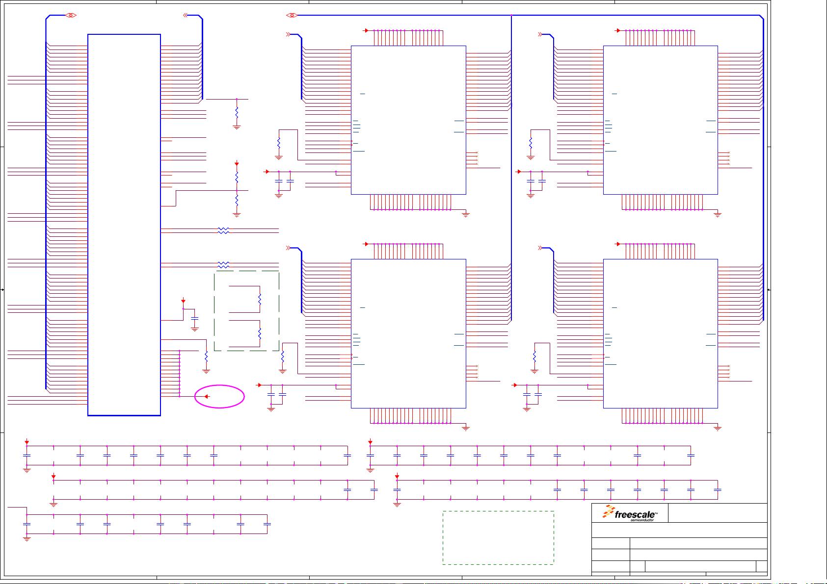
Memory <DDR3>
MX6Q MISCI
MX6Q MISCII
eMMC
USB OTG/HOST
HDMI
LCD <LVDS IF>
SATA/PCIe/RGMII/LVDS
CONFIG
Audio Codec
SENSOR
SYS PWR
Charger
DDR3 PWR
Table of Content
Cover
Block Diagram
Page 1
Page 2
Page 3
Page 4
Page 5
Page 6
Page 7
Page 8
Page 9
Page 10
Page 11
Page 12
Page 13
Page 14
Page 15
Page 16
Page 17
Page 18
Page 19
Page 20
Page 21
Revision History
Rev. Code Date DescriptionBy
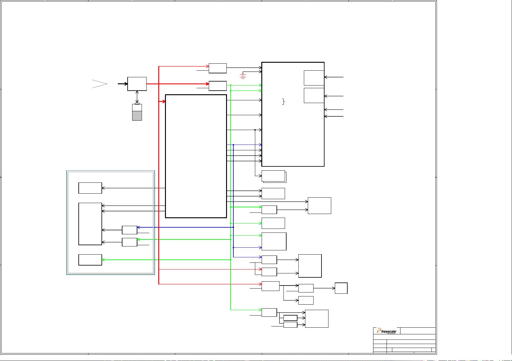
i.MX6x TV BOX Solution
Page 22
MAIN-IO CONNECTOR
1. Unless Otherwise Specified:
All resistors are in ohms, 10%, 1/8 Watt,0603
All capacitors are in uF, 20%, 50V,0603
All voltages are DC
All polarized capacitors are aluminum electrolytic
2. Interrupted lines coded with the same letter or letter
combinations are electrically connected.
3. Device type number is for reference only. The number
varies with the manufacturer.
4. Special signal usage:
_B Denotes - Active-Low Signal
<> or [] Denotes - Vectored Signals
5. Interpret diagram in accordance with American
National Standards Institute specifications, current
revision, with the exception of logic block symbology.
PCIe
Page 23
Page 24
Page 25
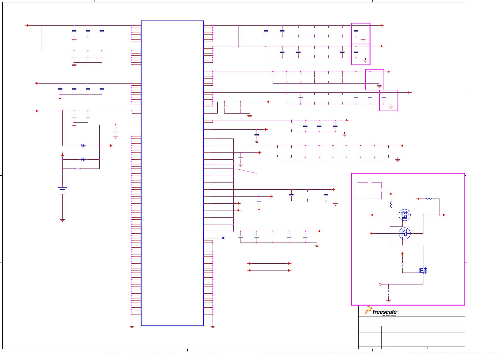
MX6Q PWR
Schematics revA DevBoard
WiFi / BT / FM
Page 26
Page 26
NOTES
Page 27
IOMUX
Page 28
PWR TREE
2012-3-15 Javen Add R1650 to support ISL8016IRAJZ DCDC PWM and PFM mode
Add D1101 for microphone signal input filter
Add Q1102 for 32K_OUT buffer
Change C1423-C1427 to 220uF/6.3V
Add Q1701,Q1702 for DDR3 suspend voltage adjustment
2 2012-3-16 Javen Add R1433-R1436 to compatible ZTE MF260A Modem PCM IF
Change R1102,R1103 pull up power to DCDC_1V8
2012-3-20 Javen Add U102 to support SDXC
Add J501 to support eMMC/MicroSD exchange
Add L706-L710 to support LVDS dual ch display
Add Q603 to backup the 1.1V power
Add Q1703 to support NVCC_DRAM power down when suspend
3
4 2012-3-24 Javen
Change U1203 L3G4200D to Invensense MPU-3050C Gyro for cost down reason
Add D401, D402, del U402 for cost down reason
Change R502-R510 pull up to VCC_EMMC3V3
Add D1503, Del Q1508, Q1510 for cost down reason
5 2012-3-27 Javen Add U1508 MCU for cost down backup
6 2012-4-4 Javen
DEL U1301 WIFI/BT/FM PWR control
Add Q101,Q102 for VP/VPH PWR control
Change U1603 ISL8016 to U1603 and U1606 MP2130
DEL C1313 C1309 C1312 according to the AMPAK's suggestion
Alan
Change XRB521S-30 to the RB520CS-30T2R
Change MMBT3904 to the PBSS2515E
DEL Reset KEY,Reserve TP
Change X402 to 32.768Khz ,Package: XTAL3215
Add MODE0 MODE1 and VDD_SNVS_IN on J301,and change J301 to 32PIN
2012-4-6
2012-4-7 Alan
DEL RP1101
Change WM8958 to MOD
Change J1501 to 50278-00701-001
Change J1801 to HDMI_BSQ-2
Change SW1501 to EVQP7C01K
2012-4-8
Alan Change the Earphone circuit,put the C1121 and C1124 close to the WM8960
Change the HP MIC circuit
2012-4-10 Alan
Change the Micro HDMI to Mini HDMI
Add R1586, R1587 for USB CHG DET
Add sleep/wake up pin for 3G modem U6300V(longshang) Del LCD_UnD and LCD_LnR
Change the Charge LED
Change the HP MIC circuitAlan2012-4-11
Add the ESD close to the ON/OFF KEY
7
8
9
10
11
12
2012-4-12
Change the micro usb connector
Change the 7'' LCD to BOE.
Compatible with the CHIMEI IPS 10.1''
Alan
Javen12 2012-4-16 Add D1510 for RTC wakeup
Add Q1606 for DVFS