没有合适的资源?快使用搜索试试~ 我知道了~
芯天下XT26G01C数据手册
需积分: 1 0 下载量 200 浏览量
2024-06-04
15:18:15
上传
评论
收藏 2.92MB PDF 举报
温馨提示
![preview](https://dl-preview.csdnimg.cn/89397712/0001-21fa1289e2087d4bdcb36a4607bf6895_thumbnail.jpeg)
![preview-icon](https://csdnimg.cn/release/downloadcmsfe/public/img/scale.ab9e0183.png)
试读
50页
芯天下XT26G01C数据手册
资源推荐
资源详情
资源评论
![pdf](https://img-home.csdnimg.cn/images/20210720083512.png)
![pptx](https://img-home.csdnimg.cn/images/20210720083543.png)
![exe](https://img-home.csdnimg.cn/images/20210720083343.png)
![pdf](https://img-home.csdnimg.cn/images/20210720083512.png)
![gz](https://img-home.csdnimg.cn/images/20210720083447.png)
![ppt](https://img-home.csdnimg.cn/images/20210720083527.png)
![none](https://img-home.csdnimg.cn/images/20210720083646.png)
![thumb](https://img-home.csdnimg.cn/images/20210720083646.png)
![rar](https://img-home.csdnimg.cn/images/20210720083606.png)
![none](https://img-home.csdnimg.cn/images/20210720083646.png)
![zip](https://img-home.csdnimg.cn/images/20210720083736.png)
![](https://csdnimg.cn/release/download_crawler_static/89397712/bg1.jpg)
Apr 18, 2020 Rev A1.0 Page 2
XT26G01C
SPI NAND
XT26G01C
3.3V 1G-BIT
SPI NAND FLASH
MEMORY
Future routine revisions will occur when appropriate, without notice. Contact XTX TECHNOLOGY
LIMITED, sales office to obtain the latest specifications and before placing your product order. Please
also pay attention to information published by XTX TECHNOLOGY LIMITED by various means, including
XTX TECHNOLOGY LIMITED. Web Site: http://www.xtxtech.com/; Technical Contact: fae@xtxtech.com
Trademarks
XTX TECHNOLOGY LIMITED name and logo, the XTX logo are trademarks or registered trademarks of
XTX TECHNOLOGY LIMITED or its subsidiaries in China. XTX TECHNOLOGY LIMITED, Printed in the
China, All Rights Reserved.
XTX Confindential
Preliminary
![](https://csdnimg.cn/release/download_crawler_static/89397712/bg2.jpg)
Apr 18, 2020 Rev A1.0 Page 3
XT26G01C
SPI NAND
CONTENTS
1.
Overview ............................................................................................................................................................................ 5
2.
Features ............................................................................................................................................................................. 5
3.
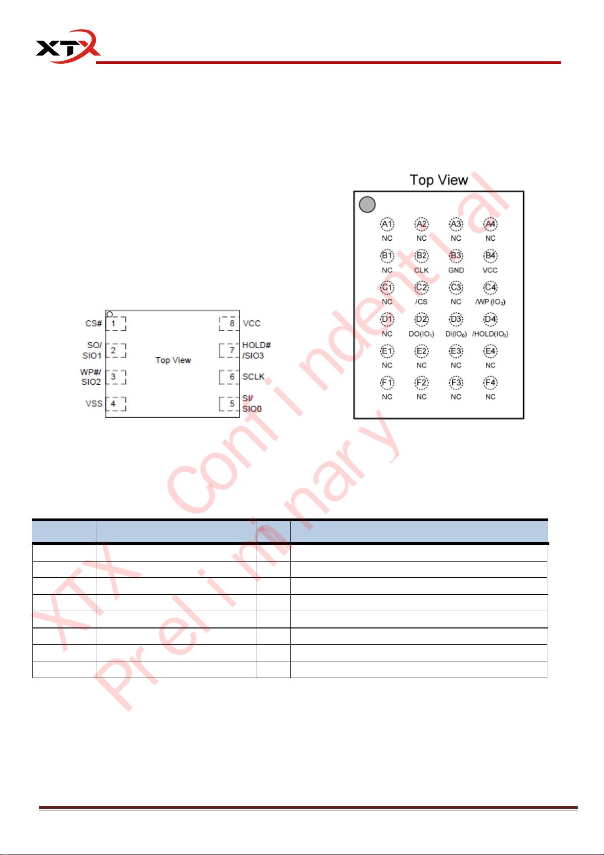
Packaging Type and Pin Configurations ............................................................................................................................. 6
4.
Block Diagram .................................................................................................................................................................... 7
5.
Memory Mapping .............................................................................................................................................................. 8
6.
Array Organization ............................................................................................................................................................. 9
7.
Device Operation ............................................................................................................................................................. 10
7.1
SPI Modes ................................................................................................................................................................ 10
Standard SPI .......................................................................................................................................................... 10 7.1.1
Dual SPI ................................................................................................................................................................. 10 7.1.2
Quad SPI................................................................................................................................................................ 10 7.1.3
7.2
Pin Description ......................................................................................................................................................... 11
CS# ........................................................................................................................................................................ 11 7.2.1
CLK ........................................................................................................................................................................ 11 7.2.2
Serial Input (SI) / SIO0 ........................................................................................................................................... 11 7.2.3
Serial Output (SO) / SIO1 ...................................................................................................................................... 11 7.2.4
Write Protect (WP#) / SIO2 ................................................................................................................................... 11 7.2.5
Hold (HOLD#) / SIO3 ............................................................................................................................................. 12 7.2.6
7.3
Command Set Tables ............................................................................................................................................... 13
7.4
WRITE
OPERATIONS ................................................................................................................................................. 15
Write Enable (WREN) (06H) .................................................................................................................................. 15 7.4.1
WRITE DISABLE (WRDI) (04h) ............................................................................................................................... 16 7.4.2
7.5
FEATURE OPERATIONS ............................................................................................................................................ 17
Get Features (0FH) and Set Features (1FH) .......................................................................................................... 17 7.5.1
7.6
READ OPERATIONS .................................................................................................................................................. 19
Page Read ............................................................................................................................................................. 19 7.6.1
Page Read to Cache (13H) .................................................................................................................................... 20 7.6.2
Read From Cache (03H or 0BH) ............................................................................................................................ 21 7.6.3
Read From Cache x2 (3BH) .................................................................................................................................... 21 7.6.4
Read From Cache x4 (6BH) ................................................................................................................................... 22 7.6.5
Read From Cache Dual IO (BBH) ........................................................................................................................... 23 7.6.6
Read From Cache Quad IO (EBH) .......................................................................................................................... 24 7.6.7
Read ID (9FH) ........................................................................................................................................................ 25
7.6.8
Read UID (4BH) ..................................................................................................................................................... 26 7.6.1
7.7
PROGRAM OPERATIONS .......................................................................................................................................... 27
Page Program ....................................................................................................................................................... 27 7.7.1
Program Load (PL)(02H)........................................................................................................................................ 28 7.7.2
XTX Confindential
Preliminary
![](https://csdnimg.cn/release/download_crawler_static/89397712/bg3.jpg)
Apr 18, 2020 Rev A1.0 Page 4
XT26G01C
SPI NAND
Program Load x4 (PL x4) (32H) ............................................................................................................................. 28
7.7.3
Program Execute (PE) (10H) ................................................................................................................................. 29 7.7.4
Internal Data Move ............................................................................................................................................... 30 7.7.5
Program Load Random Data (84H) ....................................................................................................................... 30 7.7.6
Program Random Data x4 (C4H/34H) ................................................................................................................... 31 7.7.7
Program Random Quad IO (72H) .......................................................................................................................... 32 7.7.8
7.8
ERASE OPERATIONS ................................................................................................................................................. 33
Block Erase (D8H) .................................................................................................................................................. 33 7.8.1
7.9
RESET OPERATIONS ................................................................................................................................................. 34
RESET (FFh) ........................................................................................................................................................... 34 7.9.1
7.10
WRITE PROTECT ..................................................................................................................................................... 35
8.
Status Register ................................................................................................................................................................. 36
9.
OTP Region ....................................................................................................................................................................... 37
9.1
OTP Access ............................................................................................................................................................... 37
9.2
OTP Protect .............................................................................................................................................................. 37
10.
Error Management ......................................................................................................................................................... 38
11.
ECC Protection ............................................................................................................................................................... 39
12.
Electrical Characteristics ................................................................................................................................................ 40
12.1
Absolute Maximum Ratings ................................................................................................................................... 40
12.2
Pin Capacitance ...................................................................................................................................................... 40
12.3
Power-on and Power-off Timing............................................................................................................................ 41
12.4
DC Electrical Characteristics .................................................................................................................................. 42
12.5
AC Measurement Conditions ................................................................................................................................. 43
12.6
AC Electrical Characteristics .................................................................................................................................. 41
13.
SPI Serial Timing ............................................................................................................................................................. 43
14.
Ordering Information ..................................................................................................................................................... 44
15.
Package Information ...................................................................................................................................................... 45
15.1
8-Pad WSON8 (8*6mm) ......................................................................................................................................... 45
15.2
24-Ball TFBGA (6*8mm) ......................................................................................................................................... 46
16.
Revision History .............................................................................................................................................................. 47
XTX Confindential
Preliminary
![](https://csdnimg.cn/release/download_crawler_static/89397712/bg4.jpg)
Apr 18, 2020 Rev A1.0 Page 5
XT26G01C
SPI NAND
1.
Overview
The XT26G01C is a 1G-bit (128M-byte) SPI (Serial Peripheral Interface) NAND Flash memory, with advanced
write protection mechanisms. The XT26G01C supports the standard Serial Peripheral Interface (SPI), Dual/Quad
I/O option.
2.
Features
1G-bit NAND Flash memory
– Single-level cell (SLC) technology
– Page size : 2176 bytes(2048 + 128 bytes)
– Block size : 64 pages(128K + 8K bytes)
– Device size: 1Gb(1024 blocks)
Serial Interface
– Standard SPI: CLK, CS#, SI, SO, WP#
– Dual SPI: CLK, CS#, SIO0, SIO1, WP#
– Quad SPI: CLK, CS#, SIO0, SIO1, SIO2, SIO3
High Performance
– 104MHz for fast read
– Quad I/O data transfer up to 416Mbits/s
– 2K-Byte cache for fast random read
Advanced Security Features
– Write protect all/portion of memory via software
– Lockable 8K-Byte OTP region
– 128-Bit Unique ID for each device
Program/Erase/Read Speed
– Page Program time : 450us typical
– BLOCK ERASE time : 4ms typical
– PAGE READ time : 120us maximum (without ECC)
Single Supply Voltage: 2.7V~3.6V
Advanced Security Features
– 8 bit ECC option, per 512 bytes
– Internal data move by page with ECC
– Promised golden block0
Package
– 8-pin WSON (8*6mm)
– 24-ball BGA (6*8mm)
– All Packages are RoHS Compliant and Halogen-free
Data retention: 10 years
XTX Confindential
Preliminary
![](https://csdnimg.cn/release/download_crawler_static/89397712/bg5.jpg)
Apr 18, 2020 Rev A1.0 Page 6
XT26G01C
SPI NAND
3.
Packaging Type and Pin Configurations
XT26G01C is offered in an 8-pin WSON 8x6 mm
2
as shown below. Package diagram and dimension are
illustrated at the end of this datasheet.
Connection Diagram Figure1.
Pin Description
PIN NO.
PIN NAME
I/O
FUNCTION
1
CS#
I
Chip Select Input
2
SO (SIO
1
)
I/O
Data Output (Data Input Output 1)
(1)(2)
3
WP# (SIO
2
)
I/O
Write Protect Input (Data Input Output 2)
(2)
4
VSS
Ground
5
SI (SIO
0
)
I/O
Data Input (Data Input Output 0)
(1)(2)
6
CLK
I
Serial Clock Input
7
HOLD# (SIO
3
)
I/O
Hold Input (Data Input Output 3)
(2)
8
VCC
Power Supply
Notes:
1. SIO0 and SIO1 are used for Dual SPI instructions.
2. SIO0 – SIO3 are used for Quad SPI instructions
XTX Confindential
Preliminary
剩余49页未读,继续阅读
资源评论
![avatar-default](https://csdnimg.cn/release/downloadcmsfe/public/img/lazyLogo2.1882d7f4.png)
![avatar](https://profile-avatar.csdnimg.cn/b1a962b0e5ba4f5d9b60488a55bbab79_emlinuxdeveloper.jpg!1)
EmLinuxDeveloper
- 粉丝: 166
- 资源: 37
上传资源 快速赚钱
我的内容管理 展开
我的资源 快来上传第一个资源
我的收益
登录查看自己的收益我的积分 登录查看自己的积分
我的C币 登录后查看C币余额
我的收藏
我的下载
下载帮助
![voice](https://csdnimg.cn/release/downloadcmsfe/public/img/voice.245cc511.png)
![center-task](https://csdnimg.cn/release/downloadcmsfe/public/img/center-task.c2eda91a.png)
最新资源
- chaxun.java
- 将自己的jar包(工具类)发布到maven仓库的教程,实测有效(20240628)
- 305建筑结构水电欧式6套(14.5x20.2)\施工图\D型施工图\空调系统示意图.dwg
- springboot集成fastjson2配置说明,fastjson1存在漏洞所以升级成fastjson2
- 基于Matlab机器人学导论课程作业,其中包括了轨迹规划,PD控制器,无外力和有外力的阻抗控制器(课程设计报告+源码)
- 305建筑结构水电欧式6套(14.5x20.2)\施工图\D型施工图\空调标高空调平面图.dwg
- 305建筑结构水电欧式6套(14.5x20.2)\施工图\D型施工图\空调08二层空调平面图(二).dwg
- 305建筑结构水电欧式6套(14.5x20.2)\施工图\D型施工图\空调07二层空调平面图(一).dwg
- 305建筑结构水电欧式6套(14.5x20.2)\施工图\D型施工图\空调06首层空调平面图(二).dwg
- 算法来增强指纹图像.zip
资源上传下载、课程学习等过程中有任何疑问或建议,欢迎提出宝贵意见哦~我们会及时处理!
点击此处反馈
![feedback](https://img-home.csdnimg.cn/images/20220527035711.png)
![feedback-tip](https://img-home.csdnimg.cn/images/20220527035111.png)
安全验证
文档复制为VIP权益,开通VIP直接复制
![dialog-icon](https://csdnimg.cn/release/downloadcmsfe/public/img/green-success.6a4acb44.png)