没有合适的资源?快使用搜索试试~ 我知道了~
AMS-AS1345A.pdf
5星 · 超过95%的资源 需积分: 9 1 下载量 97 浏览量
2022-11-12
14:18:11
上传
评论 1
收藏 861KB PDF 举报
温馨提示
试读
31页
AMS-AS1345A.pdf
资源详情
资源评论
ams Datasheet Page 1
[v1-56] 2016-Dec-28 Document Feedback
AS1345
18V, High Efficiency, DC/DC Step-Up
Converter
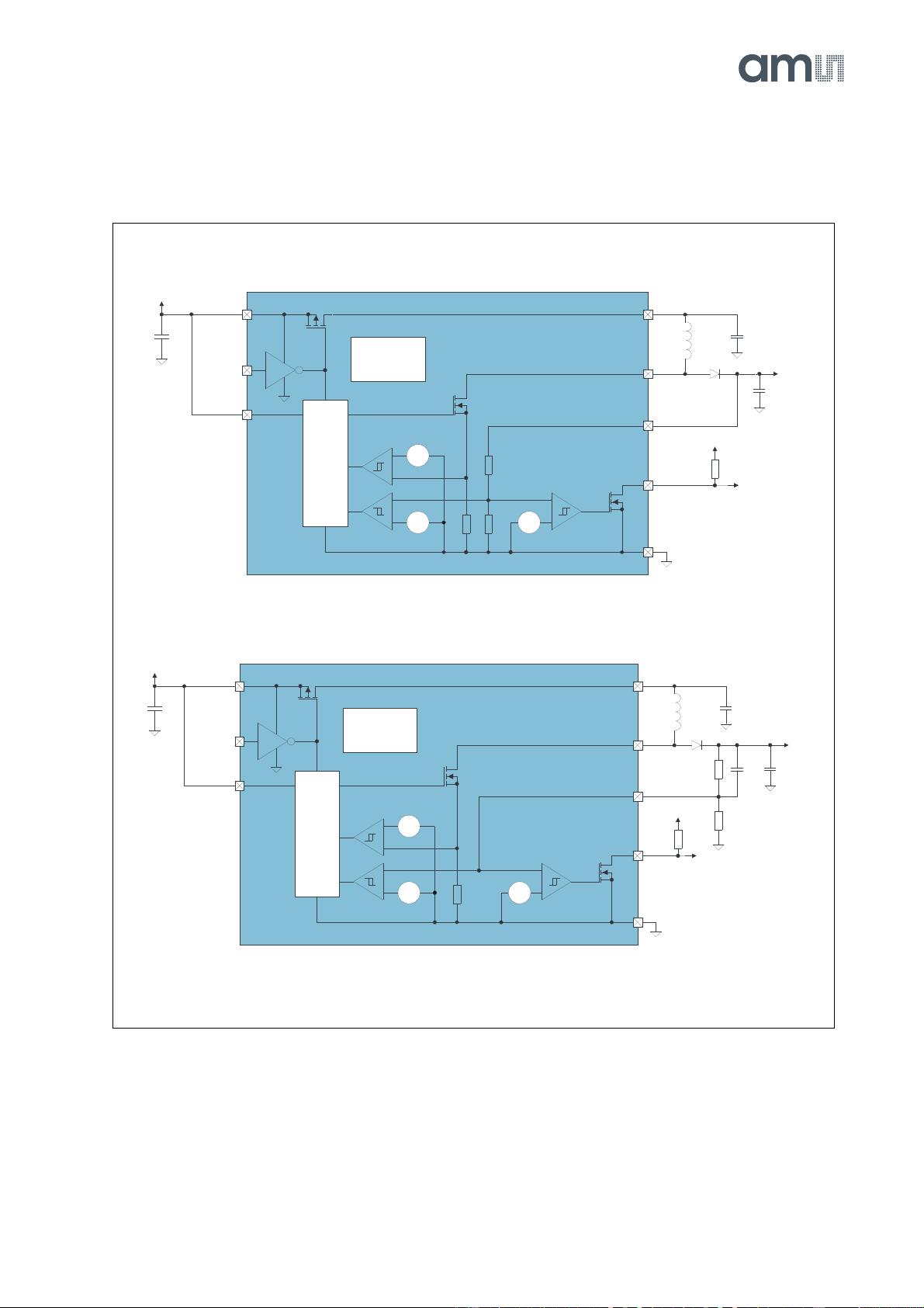
The AS1345 high efficiency DC/DC step-up converter contains
an internal N-channel and an internal P-channel output
isolation switch.
The device operates from a 2.9V to 5.0V supply and can boost
voltages up to 18V.
A hysteretic control scheme is used to provide the highest
operating efficiency over a wide range of input and output load
conditions. The internal MOSFET switches reduce the external
component count and a high switching frequency allows the
use of tiny surface mount components.
The AS1345 employ a factory set current limit to reduce ripple
and external component size in low output current
applications. With a 500mA current limit the AS1345 is capable
of providing 20mA @ 18V output.
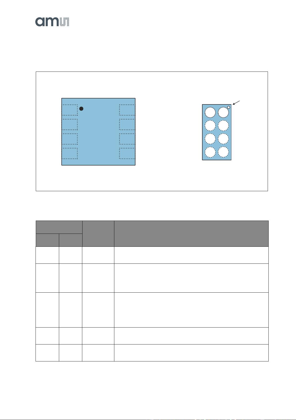
Figure 1:
Available Products
Built-in safety features protect the internal switches and output
components from fault conditions. Additional power-saving
attributes include a very low quiescent current and a true
shutdown mode.
Ordering Information and Content Guide appear at end of
datasheet.
Devices Peak Coil Current Output
AS1345A 100mA Adjustable or fixed
AS1345B 200mA Adjustable or fixed
AS1345C 350mA Adjustable or fixed
AS1345D 500mA Adjustable or fixed
General Description
Page 2 ams Datasheet
Document Feedback [v1-56] 2016-Dec-28
AS1345 − General Description
Key Benefits & Features
The benefits and features of AS1345, 18V, High Efficiency,
DC/DC Step-Up Converter are listed below:
Figure 2:
Added Value of Using AS1345
Applications
The AS1345 is ideal for:
• Small and low current demand LCD panels as well as for
polymer LEDs (OLED)
• Cell phones, PDAs
• Readers
• Mobile terminals
• 3D shutter glasses
Benefits Features
• Supports Lithium primary and re-chargeable
batteries
• Input Voltage Range: 2.9V to 5.0V
• Supports a variety of end applications
• Adjustable Output Voltage Range: 5.0V to 18V
• Output Current up to 40mA
• Allows optimization of circuit depending on
output power demands
• Inductor Peak Currents: 100, 200, 350 and 500 mA
• Battery life improved • 90% Efficiency
• Battery supply isolated during shutdown • True Shutdown
• Fault tolerant • Short Circuit and Thermal Protection
• Small chipscale package
• Packages:
• 8-pin (2x2mm) TDFN
• 8-bumps (1.570mm x 0.895mm) WL-CSP
with 0.4mm pitch
ams Datasheet Page 3
[v1-56] 2016-Dec-28 Document Feedback
AS1345 − General Description
Block Diagram
The functional blocks of this device are shown below:
Figure 3:
AS1345 Block Diagram
Driver
&
Control
Logic
Die
Temperature
Monitor
SWIN
EN
VDD
LX
SWOUT
GND
ILIM
+
+
1.25V
AS1345
1
0
u
H
D
1
10uF
1
.
1
2
5
V
+
P
O
K
1
0
u
F
1
u
F
t
o
1
0
u
F
P
O
K
+
-
+
-
+
-
VDD = 2.9V to 5.0V
F
B
V
D
D
V
o
u
t
=
5
.
0
V
t
o
1
8
V
1
0
0
k
Driver
&
Control
Logic
Die
Temperature
Monitor
SWIN
EN
VDD
LX
SWOUT
GND
ILIM
+
+
1.25V
AS1345
1
0
u
H
D
1
10uF
1
.
1
2
5
V
+
P
O
K
1
0
u
F
1
u
F
t
o
1
0
u
F
P
O
K
+
-
+
-
+
-
VDD = 2.9V to 5.0V
F
B
V
D
D
V
o
u
t
=
5
.
0
V
t
o
1
8
V
4
7
p
F
R
2
R
3
1
0
0
k
Fixed Output Voltage
Adjustable Output Voltage
Page 4 ams Datasheet
Document Feedback [v1-56] 2016-Dec-28
AS1345 − Pin Assignment
Figure 4:
Pin Diagram (Top View)
Figure 5:
Pin Description
Pin Number
Pin Name Description
TDFN WLP
1A1 VDD
Supply Voltage. Connect to a 2.9V to 5.0V input supply. Bypass this pin
with a 10μF capacitor.
2A2 EN
Enable Pin. Logic controlled shutdown input, 1.8V CMOS compatible;
1 = Normal operation
0 = Shutdown
On request a 100kΩ pull-down resistor can be enabled (factory set).
3A3 FB
Feedback Pin. Feedback input to the gm error amplifier.
For an adjustable output voltage connect a resistor divider to this pin.
The output can be adjusted from 5.0V to 18V by:
V
OUT = VREF x (1 + R2/R3)
If the fixed output voltage version is used, connect this pin to V
OUT.
4A4 POK
POK. Open Drain Output. POK remains low while V
OUT is less than 90%
of nominal V
OUT. Connect a 100kΩ pull-up resistor from this pin to VDD.
5B4SWIN
Shutdown Disconnect Switch In. Input pin of the internal P-channel
MOSFET.
Pin Assignment
1
2
3
4
AS1345
TDFN 8-pin
2x2mm
LX
GNDVDD
EN
FB
POK
SWOUT
SWIN
A1
VDD
B3
SWOUT
A4
POK
A3
FB
A2
EN
B2
LX
B1
GND
Pin A1
indicator
B4
SWIN
8
7
6
5
ams Datasheet Page 5
[v1-56] 2016-Dec-28 Document Feedback
AS1345 − Pin Assignment
6B3SWOUT
Shutdown Disconnect Switch Out. Output pin of the internal
P-channel MOSFET. Connect to power inductor and decouple to GND
with a 10μF low ESR ceramic capacitor.
When the input disconnect feature is not desired, SWOUT should be
connected to SWIN and VDD.
7B2 LX
Inductor. The drain of the internal N-channel MOSFET. Connect to
power inductor and to anode of a schottky diode.
8B1 GNDGround
Pin Number
Pin Name Description
TDFN WLP
剩余30页未读,继续阅读
安全验证
文档复制为VIP权益,开通VIP直接复制
信息提交成功
评论1
最新资源