没有合适的资源?快使用搜索试试~ 我知道了~
TOSHIBA东芝 TB6605FTG-datasheet产品规格书.pdf
需积分: 0 0 下载量 65 浏览量
2024-06-05
13:20:56
上传
评论
收藏 1.26MB PDF 举报
温馨提示
TB6605FTG的先进特性为工程师带来了诸多实际应用中的好处: 1. **高效节能**:采用低导通电阻的DMOS FET意味着在工作中产生的热量更少,不仅提高了效率,还减少了对大型散热解决方案的需求。这在空间有限且热管理至关重要的应用中尤为有利。 2. **简化设计**:集成的预驱动电路大大简化了电机控制设计。工程师可以将更多精力放在优化项目的其他方面,而不必担心传统电机驱动器所需的额外电路。 3. **增强的可靠性**:热关断电路和宽工作温度范围确保了TB6605FTG即使在恶劣条件和长时间使用下也能保持稳定性能。这使其成为工业应用中对可靠性要求较高场景的理想选择。 4. **应用广泛**:无论是机器人、自动化设备还是消费电子产品,TB6605FTG都具备灵活性,能够适应多种电机控制需求。其坚固的设计和全面的特性使其成为工程师工具箱中的一项重要资源。
资源推荐
资源详情
资源评论

TB6605FTG
1
2
3
4
5 6 7 8
9
10
11
12
13
14
15
16
17
18
19 20 21
22
23 24 25 26 27
28
29
30
31
32
33
34
35
36
HA+
HA-
HB+
HB-
HC+
HC-
CLd
OSC_C
OSC_R
Dif_in
LA
FV
TCR
HP
Vreg
CW/CCW
BRAKE
PWM_in
START
Soft-C
CP2
OVP
CP1
CP3
VCC
GND
Idc
LA(U)
OUT-A
LA(L)
LB(U)
OUT-B
LB(L)
LC(U)
OUT-C
LC(L)
TOSHIBA Bi-CMOS Integrated Circuit Silicon Monolithic
TB6605FTG
3-phase Full-wave Sine-wave Brushless Motor Controller
TB6605FTG is a 3-phase full-wave sine-wave PWM brushless motor
control IC.东芝代理,大量现货:QQ 990123167 13610068393
Sine-wave PWM driving with 2-phase modulation enables driving
in high efficiency and low noise condition.
Features
• Sine-wave PWM driving system
• 2-phase modulation system with low switching loss
• Upper Nch – Lower Nch FET
• Dead time function included
• Brake function included
• Start function included
• Speed command: PWM input type
• Auto lead-angle control function included
(Lead angle is set based on the speed)
• CW/CCW function included
• Lock protection function included
• Output signal of hall pulse monitor included
Weight: 0.08 g (typ.)
P-VQFN36-0505-0.50-001
This
product has a MOS structure and is sensitive to electrostatic discharge. When handling this product, ensure that the
environment is protected against electrostatic discharge by
using an earth strap, a conductive mat and an ionizer. Ensure
also that the ambient temperature and relative humidity are maintained at reasonable levels.
The IC should be installed correctly. Otherwise, the IC or peripheral parts and devices may be degra
ded or permanently
damaged.
©2015 TOSHIBA Corporation 2015-04-23
1 / 24

TB6605FTG
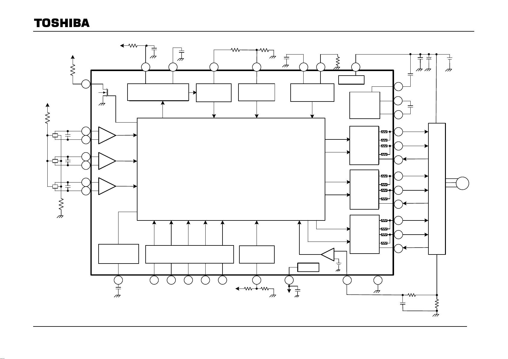
1.1.1. Block Diagram
Some of the functional blocks, circuits, or constants in the block diagram may be omitted or simplified for explanatory purposes.
1
2
3
4
5
6
R1
VCC
R2
C1
C2
C3
HA+
HA-
HB+
HB-
HC+
HC-
11
R9
チャージ
ポンプ
Vreg
5V
C7
17
27
CW
/CCW
Idc
プリ
ドライバ
8V
8
9
OSC_C
OSC_R
26 GND
25 VCC
28
30
C9
C10
+
-
(24V)
LA(U)
LA(L)
M
R6
R5
C6
R7
C11
C12
13
TCR
15
C5
20
C4
CLd
7
OVP
22
19
START BRAKE
Dif-inLA
進角設定
AD変換
12
18
PWM-in
14
HP
FV変換回路
16
FV
速度帰還
AD変換
ソフトスタート
入力回路
ロック保護
AD変換
内部基準
クロック
Nch
+
Nch
29
プリ
ドライバ
31
33
LB(U)
LB(L)
32
プリ
ドライバ
34
36
LC(U)
LC(L)
35
24
21
23
10
Vreg
R11
Vreg
Vreg
OUT-A
OUT-B
OUT-C
CP1
CP2
CP3
R3 R4
C8
C13
R8
R10
Soft-C
正弦波制御回路
FV convertor circuit
Lead angle
set
AD convertor
Internal
reference
clock
Charge
pump
Pre-driver
Pre-driver
Pre-driver
Lock
protection
AD convertor
Soft start
Input circuit
Sine-wave controller
Speed
feedback
AD convertor
©2015 TOSHIBA Corporation 2015-04-23
2 / 24
东芝代理,大量现货:QQ 990123167 13610068393

TB6605FTG
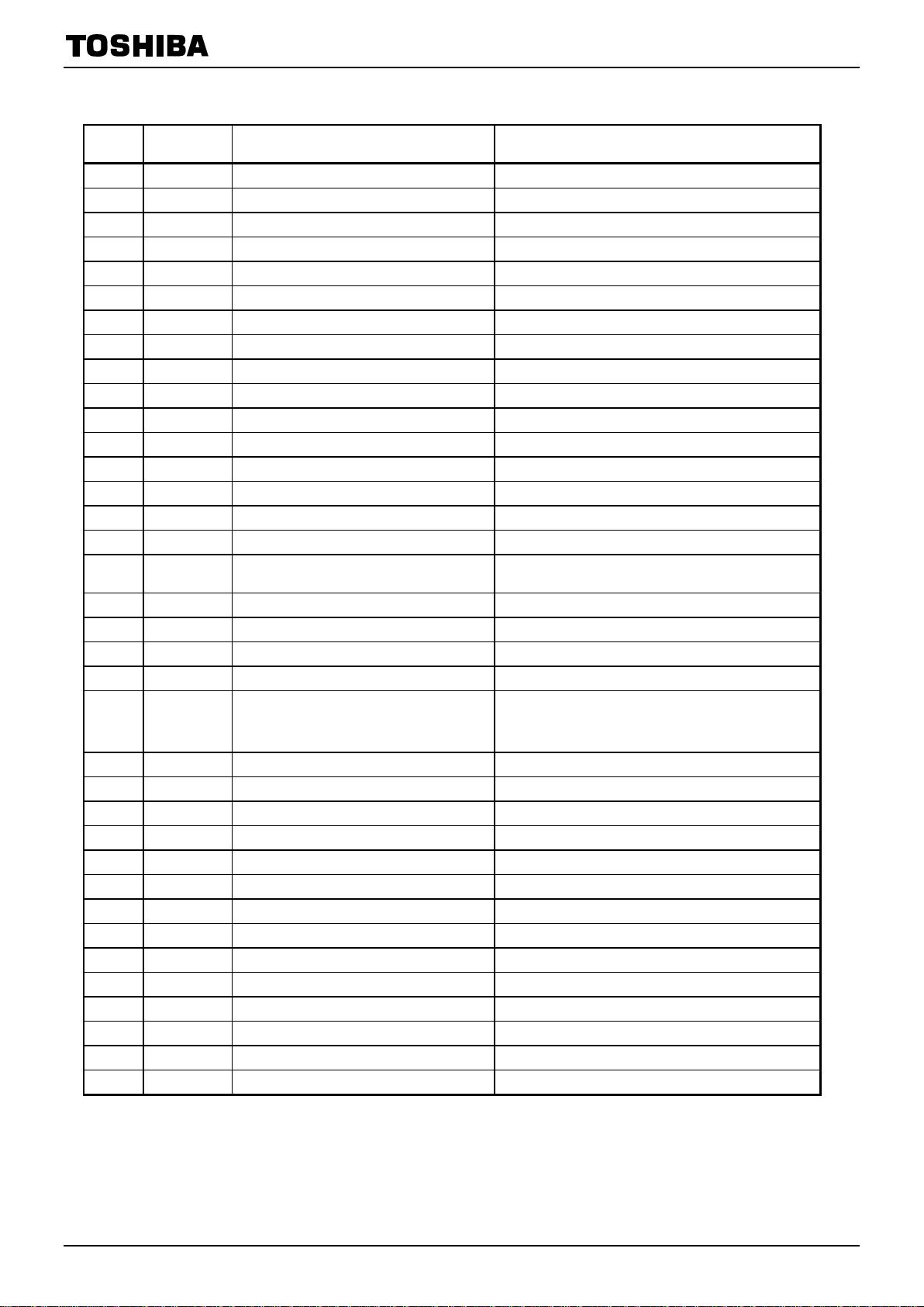
1.1.2. Pin Description
No. Name Description Note
1 HA+ Hall signal (Phase-A +) input Hall element (Phase-A) signal + input
2 HA- Hall signal (Phase-A -) input Hall element (Phase-A) signal - input
3 HB+ Hall signal (Phase-B +) input Hall element (Phase-B) signal + input
4 HB- Hall signal (Phase-B -) input Hall element (Phase-B) signal - input
5 HC+ Hall signal (Phase-C +) input Hall element (Phase-C) signal + input
6 HC- Hall signal (Phase-C -) input Hall element (Phase-C) signal - input
7 CLd Lock protection circuit setting pin Voltage input
8 OSC_C Internal reference clock setting C connecting External capacitor between GND and OSC_C.
9 OSC_R Internal reference clock setting R connecting External resistor between GND and OSC_R.
10 Dif_in Speed feedback input -
11 LA Lead angle setting voltage input Input lead angle ADC
12 FV Smoothing pin of MMV output External capacitor
13 TCR CR pin of MMV External resistor and capacitor
14 HP Output signal of hall pulse monitor HA monitor of signal after it makes it to binary
15 Vreg 5V Power voltage source Connecting capacitor to GND against 5 V output
16 CW/CCW CW/CCW switching pin H: Reverse/L: Forward, Pull up resistor of 50 kΩ (typ.)
17 BRAKE Brake signal input L: Brake (All phases of lower side:
ON), Pull up resistor of
50 kΩ (typ.)
18 PWM_in PWM signal input for speed command Pull up resistor of 50 kΩ (typ.)
19 START Start signal input L: Start, H: Stop, Pull up resistor of 50 kΩ (typ.)
20 Soft-C Capacitor pin for soft start External capacitor
21 CP2 Charge pump 2 For upper side Nch FET gate voltage
22 OVP Switching pin for avoiding voltage booster Pull up resistor of 50 kΩ (typ.)
TEST pin is held concurrently,
TEST mode: Vref + 0.7 V (= 5.7 V) or more
23 CP1 Charge pump 1 For upper side Nch FET gate voltage
24 CP3 Charge pump 3 For upper side Nch FET gate voltage
25 VCC Logic Supply voltage pin V
CC
(opr.) = 9 to 28 V
26 GND Ground pin -
27 Idc Output current detection signal input pin Into gate block function when over 0.25 V (typ.)
28 LA (U) Phase-A driving signal output (U) Phase-A output FET gate (for upper-side Nch)
29 OUT-A Phase-A motor pin -
30 LA (L) Phase-A driving signal output (L) Phase-A output FET gate (for lower-side Nch)
31 LB (U) Phase-B driving signal output (U) Phase-B output FET gate (for upper-side Nch)
32 OUT-B Phase-B motor pin -
33 LB (L) Phase-B driving signal output (L) Phase-B output FET gate (for lower-side Nch)
34 LC (U) Phase-C driving signal output (U) Phase-C output FET gate (for upper-side Nch)
35 OUT-C Phase-C motor pin -
36 LC (L) Phase-C driving signal output (L) Phase-C output FET gate (for lower-side Nch)
** Metal exposed part on the 4 corners and the underside are connected electrically each other.
Although pin assignment is considered to avoid the distraction from pin-pin or pin-metal area shortage, use in the state of the
metal area on 4 corners and underside is opened electrically.
(If connected to ground, there is a possibility for distraction with shortage.)
©2015 TOSHIBA Corporation 2015-04-23
3 / 24

TB6605FTG
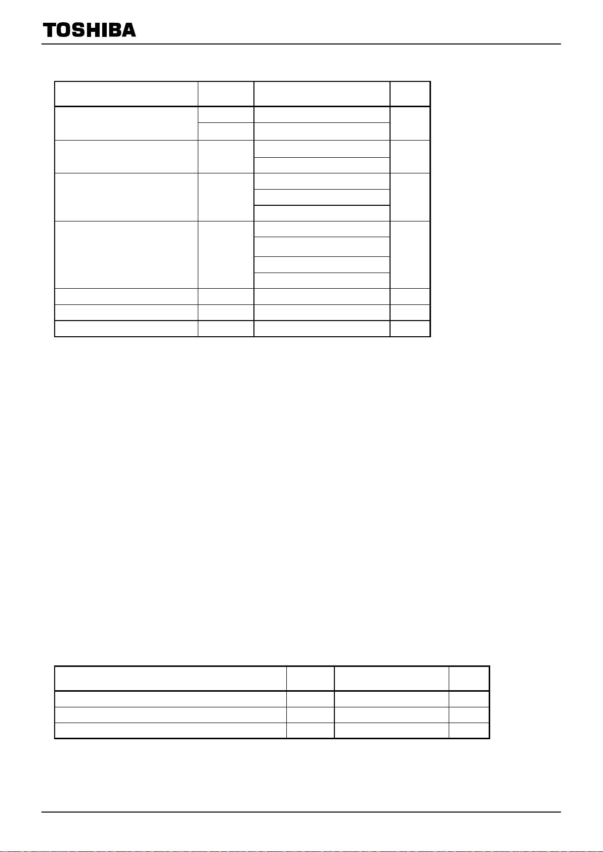
1.1.3. Absolute maximum ratings (Ta = 25°C)
Characteristics Symbol Rating Unit
Supply voltage
V
CC
1
30 (Note. 1)
V
V
CC
2 32 (Note. 2)
Input voltage V
IN
5.5 (Note. 3)
V
Vreg (Note. 4)
Output voltage V
OUT
5.5 (Note. 5)
V
30 (Note. 6)
40 (Note. 7)
Output current I
OUT
10 (Note. 8)
mA
20 (Note. 9)
10 (Note. 10)
2 (Note. 11)
Power dissipation P
D
1.56 (Note. 12) W
Operation temperature T
opr
−30 to 85 °C
Storage temperature T
stg
−55 to 150 °C
Note 1: Vcc (in normal operation)
Note 2: Vcc (When 8 V charge pump is disabled, without external C for the charge pump)
* In normal operation, absolute maximum rating is Vcc1, as charge pump function is necessary for the operation.
Note. 3: CW/CCW, START, BRAKE, and PWM-in
Note. 4: OVP
Note. 5: HP
Note. 6: OUT-A, OUT-B, and OUT-C
Note. 7: LA (U), LB (U), and LC (U)
Note. 8: LA(U),LB(U),LC(U), LA(L),LB(L), and LC(L) source current
Note. 9: LA(U),LB(U),LC(U), LA(L),LB(L), and LC(L) sink current
Note. 10: Vreg
Note. 11: HP
Note. 12: Mounted on PCB (Glass epoxy 76.2 mm × 114.3 mm × 1.6 mm, Cu area 60 %, single layer)
Absolute maximum rating is the standard without any exception even in a moment.
If the IC is operated in a condition beyond the rating, destruction, degeneration or damaging of IC or external parts possibly
occurs. Design to avoid the condition beyond the rating in any operating condition.
Operate within the condition described in next table “Operating condition”.
1.1.4. Operating condition (Ta = 25°C)
Characteristics Symbol Rating Unit
Supply voltage (Note. 1) V
CC
9 to 28 V
PWM input signal for speed command (PWM_in) (Note. 2) PWM_in 10 to 100 kHz
Internal reference clock frequency (Note. 3) fx 2 to 8 MHz
(Note. 1): OUT-A, OUT-B, and OUT-C pins should be rating voltage (30 V) or less.
(Note. 2): Output PWM frequency does not change depending on PWM-in frequency.
Output PWM is configured depending on the internal reference clock frequency.
(Note. 3): Please configure the external constant number including variation.
©2015 TOSHIBA Corporation 2015-04-23
4 / 24

TB6605FTG
1.1.5. Description for operation
1. Sine-wave PWM driving
1.1.5.1. < Energization mode switching >
When starting, TB6605FTG operates rectangle driving of 120° energization signal with position detect signal.
After f (frequency every 1 phase of position detect signal (hall element signal)) goes beyond fH (setting frequency), at HA
falling timing next-after IC counts 6 times of hall signal switching edges, the operation mode is switched to 180° energization
mode.
(About Hall input signal, see 8. Hall amplifier circuit.)
The Setting Frequency fH is determined as next.
Setting frequency: fH = fx ÷ (2
10
× 64 × 6)
The fx is internal reference clock determined with OSC_R and OSC_C.
When fx = 4 MHz, fH = 10.15 Hz,
fx = 5 MHz, fH = 12.7 Hz, and
fx = 6 MHz, fH = 15.25 Hz.
1.1.5.2. (Mode Table)
Rotating state Driving mode
f
H
> f Rectangle driving (120° energization)
f
H
< f Sinusoidal wave PWM driving (180°energization)
*To avoid malfunction from noise, IC operates in 120° energization mode when f is higher than normal possible frequency.
(When fx = 5 MHz, if over 1 kHz, IC operates in rectangle 120° energization mode.)
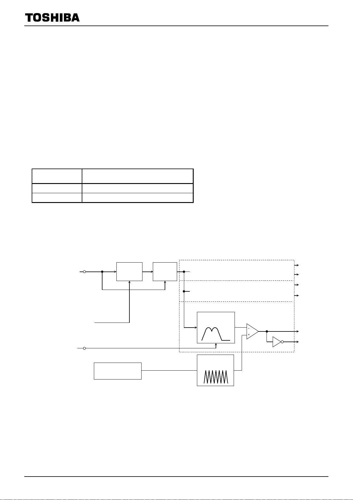
<Operation Flow>
The following figure is actually processed digitally with the image chart in the IC.
<180° energization >
●60° modulation-60° reset is operated.
The modulation signal is created from position detect signal. Sinusoidal PWM signal is created from comparing this
modulation wave to triangular wave.
IC counts the time between one zero-cross timing to next zero-cross timing of 3 position detect signals (60° electrical
angle), and use this time as next 60° phase length.
The 60° phase length of the modulation signal is from 32 data, and time length for 1 data is 1/32 of time length of the
previous 60° phase length, so modulation wave advances with this length.
Sine-wave pattern
(modulation signal)
Trianglar wave
(Carrier signal)
Position
estimation
Counter
Internal reference
clock generate
Phase
alignment
( Phase-A,
Phase-B,
Phase-C)
Position signal
Speed control
signal
Comparator
Phase-C
Phase
-B
Phase
-A
LA
(U)
LA (L)
LB
(U)
LB
(L)
LC
(U)
LC
(L)
Internal reference clock
©2015 TOSHIBA Corporation 2015-04-23
5 / 24
剩余23页未读,继续阅读
资源评论

普通网友
- 粉丝: 562
- 资源: 64
上传资源 快速赚钱
 我的内容管理
展开
 我的资源
快来上传第一个资源
 我的收益 登录查看自己的收益
 我的积分
登录查看自己的积分
 我的C币
登录后查看C币余额
 我的收藏
我的收藏  我的下载
我的下载  下载帮助
下载帮助

 前往需求广场,查看用户热搜
最新资源
- 培训与开发.ppt
- 人力资源规划培训教材(PPT 44页).ppt
- 培训制度的体系与实施.ppt
- 2016年某某铸造有限责任公司职工安全培训计划及管理办法(DOC 9页).doc
- 如何作一次完美的培训.ppt
- 2016年酒店员工培训计划方案.doc
- 如何设计年度培训计划与预算方桉.ppt
- 如何设计年度培训计划.ppt
- 2016年度公司培训计划方案-.doc
- 2016年员工培训计划方案.doc
- 2016年企业员工培训计划制定流程方案(DOC 15页).doc
- 2016年深圳童乐饰品有限公司人力资源管理程序-公司年度培训计划表(DOC 12页).doc
- 百仕瑞集团—2015年度员工培训规划方案(DOC 7页).doc
- XX公司2016年培训方案(DOC 19页).doc
- 某集团公司年度员工培训规划方案(DOC 10页).doc
- 年度员工培训规划方案.doc
资源上传下载、课程学习等过程中有任何疑问或建议,欢迎提出宝贵意见哦~我们会及时处理!
点击此处反馈


安全验证
文档复制为VIP权益,开通VIP直接复制
 信息提交成功