没有合适的资源?快使用搜索试试~ 我知道了~
ADI AD8315 50 dB GSM PA Controller
需积分: 1 0 下载量 178 浏览量
2024-01-23
10:39:03
上传
评论
收藏 552KB PDF 举报
温馨提示
试读
24页
ADI AD8315 50 dB GSM PA Controller
资源推荐
资源详情
资源评论
50 dB GSM PA Controller
AD8315
Rev. C
Information furnished by Analog Devices is believed to be accurate and reliable. However, no
responsibility is assumed by Analog Devices for its use, nor for any infringements of patents or other
rights of third parties that may result from its use. Specifications subject to change without notice. No
license is granted by implication or otherwise under any patent or patent rights of Analog Devices.
Trademarks and registered trademarks are the property of their respective owners.
One Technology Way, P.O. Box 9106, Norwood, MA 02062-9106, U.S.A.
Tel: 781.329.4700 www.analog.com
Fax: 781.461.3113 ©2006 Analog Devices, Inc. All rights reserved.
FEATURES
Complete RF detector/controller function
>50 dB range at 0.9 GHz (−49 dBm to +2 dBm, re 50 Ω)
Accurate scaling from 0.1 GHz to 2.5 GHz
Temperature-stable linear-in-dB response
Log slope of 23 mV/dB, intercept at −60 dBm at 0.9 GHz
True integration function in control loop
Low power: 20 mW at 2.7 V, 38 mW at 5 V
Power-down to 10.8 μW
APPLICATIONS
Single, dual, and triple band mobile handset (GSM, DCS, EDGE)
Transmitter power control
GENERAL DESCRIPTION
The AD8315 is a complete low cost subsystem for the precise
control of RF power amplifiers operating in the frequency range
0.1 GHz to 2.5 GHz and over a typical dynamic range of 50 dB.
It is intended for use in cellular handsets and other battery-
operated wireless devices. The log amp technique provides a
much wider measurement range and better accuracy than
controllers using diode detectors. In particular, its temperature
stability is excellent over a specified range of −30°C to +85°C.
Its high sensitivity allows control at low signal levels, thus
reducing the amount of power that needs to be coupled to
the detector.
For convenience, the signal is internally ac-coupled. This
high-pass coupling, with a corner at approximately 0.016 GHz,
determines the lowest operating frequency. Therefore, the
source can be dc grounded.
The AD8315 provides a voltage output, VAPC, that has the
voltage range and current drive to directly connect to most
handset power amplifiers’ gain control pin. VAPC can swing
from 250 mV above ground to within 200 mV below the supply
voltage. Load currents of up to 6 mA can be supported.
The setpoint control input is applied to the VSET pin and has
an operating range of 0.25 V to 1.4 V. The associated circuit
determines the slope and intercept of the linear-in-dB
measurement system; these are nominally 23 mV/dB and
−60 dBm for a 50 Ω termination (−73 dBV) at 0.9 GHz.
Further simplifying the application of the AD8315, the input
resistance of the setpoint interface is over 100 MΩ, and the bias
current is typically 0.5 μA.
The AD8315 is available in MSOP and LFCSP packages and
consumes 8.5 mA from a 2.7 V to 5.5 V supply. When powered
down, the sleep current is 4 μA.
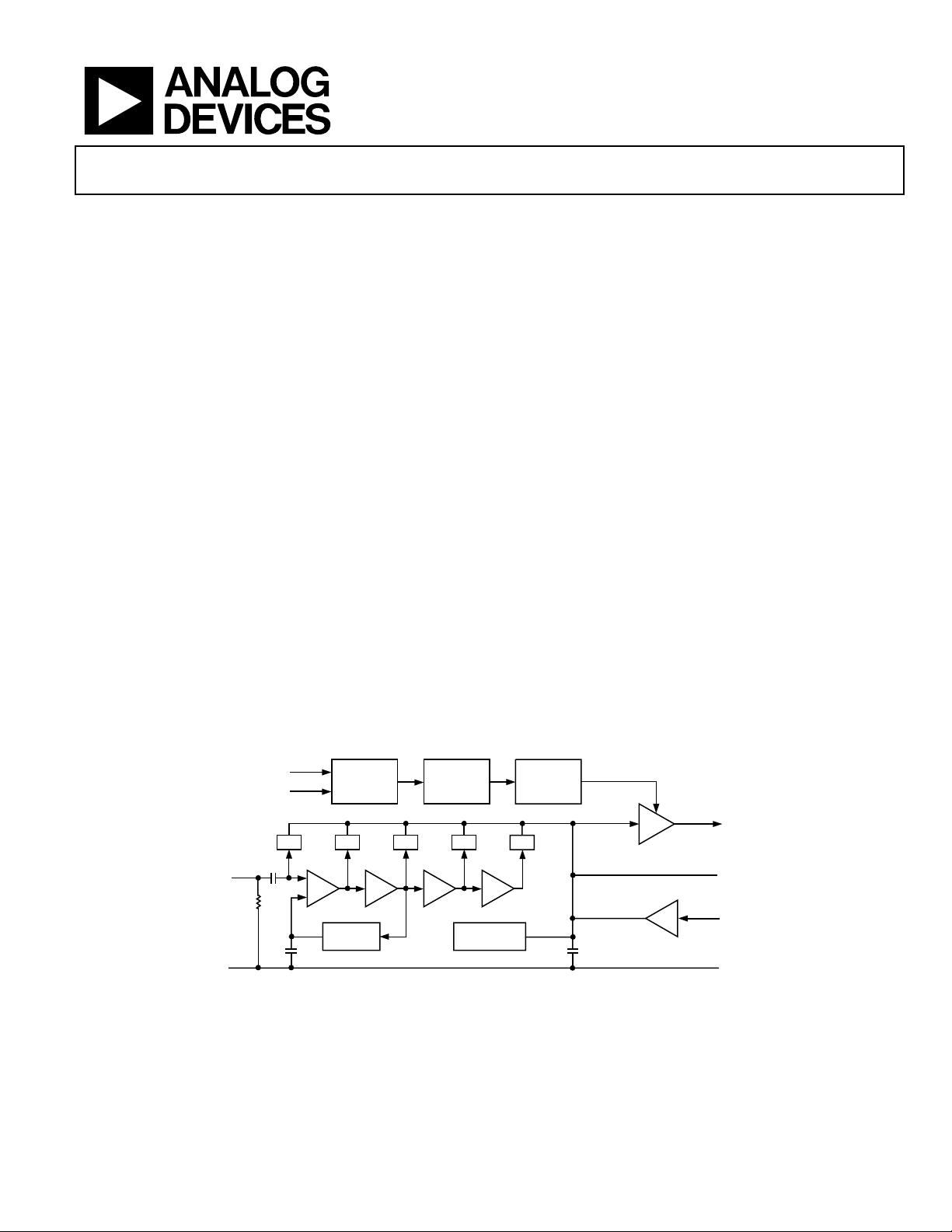
FUNCTIONAL BLOCK DIAGRAM
VPOS
ENBL
RFIN
C
OMM
DET
10dB
DET
10dB
DET DET DET
10dB 10dB
OFFSET
COMP’N
INTERCEPT
POSITIONING
LOW NOISE
GAIN BIAS
LOW NOISE
BAND GAP
REFERENCE
OUTPUT
ENABLE
DELAY
×1.35
VAPC
HI-Z
LOW NOISE (25nV/√Hz)
RAIL-TO-RAIL BUFFER
FLTR
VSET
V-I
23mV/dB
250mV TO
1.4V = 50dB
01520-001
Figure 1.
AD8315
Rev. C | Page 2 of 24
TABLE OF CONTENTS
Features .............................................................................................. 1
Applications....................................................................................... 1
General Description ......................................................................... 1
Functional Block Diagram .............................................................. 1
Revision History ............................................................................... 2
Specifications..................................................................................... 3
Absolute Maximum Ratings............................................................ 5
ESD Caution.................................................................................. 5
Pin Configuration and Function Descriptions............................. 6
Typical Performance Characteristics ............................................. 7
Theory of Operation ...................................................................... 12
Basic Theory................................................................................ 12
Controller-Mode Log Amps ..................................................... 13
Control Loop Dynamics............................................................ 13
Practical Loop............................................................................. 15
A Note About Power Equivalency ........................................... 16
Basic Connections...................................................................... 16
Range on VSET and RFIN ........................................................ 17
Transient Response .................................................................... 17
Mobile Handset Power Control Example ............................... 18
Enable and Power-On................................................................ 19
Input Coupling Options ............................................................ 19
Using the Chip Scale Package................................................... 20
Evaluation Board ........................................................................ 20
Outline Dimensions ....................................................................... 22
Ordering Guide .......................................................................... 23
REVISION HISTORY
6/06—Rev. B to Rev. C
Updated Format..................................................................Universal
Changes to Ordering Guide .......................................................... 23
1/03—Rev. 0 to Rev. B
Edits to Product Description Section ............................................ 1
Edit to Functional Block Diagram ................................................. 1
Edits to Specifications ...................................................................... 2
Edits to Absolute Maximum Ratings ............................................. 3
Ordering Guide Updated................................................................. 3
TPC 9 Replaced with New Figure .................................................. 5
Edits to TPC 27................................................................................. 8
Edit to Figure 1.................................................................................. 9
Edit to Figure 3................................................................................ 10
Edit to Equation 9........................................................................... 10
Edit to Equation 10......................................................................... 10
Edit to Equation 11......................................................................... 10
Edits to Example section ............................................................... 10
Edit to Basic Connections Section ............................................... 12
Edits to Input Coupling Options Section.................................... 14
Table III Becomes Table II............................................................. 15
Table II Recommended Components Deleted ........................... 15
Using the Chip-Scale Package Section Added............................ 15
Edits to Evaluation Board Section................................................ 15
Figure 12 Title Edited..................................................................... 16
Figure 13 Title Edited..................................................................... 16
8-Lead Chip Scale Package (CP-8) Added.................................. 17
Updated Outline Dimensions....................................................... 17
10/99—Revision 0: Initial Version
AD8315
Rev. C | Page 3 of 24
SPECIFICATIONS
V
S
= 2.7 V, T = 25°C, 52.3 Ω termination on RFIN, unless otherwise noted.
Table 1.
Parameter Conditions Min Typ Max Unit
OVERALL FUNCTION
Frequency Range
1
To meet all specifications 0.1 2.5 GHz
Input Voltage Range ±1 dB log conformance, 0.1 GHz −57 −11 dBV
Equivalent dBm Range −44 +2 dBm
Logarithmic Slope
2
0.1 GH 21.5 24 25.5 mV/dB
Logarithmic Intercept
2
0.1 GHz −79 −70 −64 dBV
Equivalent dBm Level −66 −57 −51 dBm
RF INPUT INTERFACE Pin RFIN
Input Resistance
3
0.1 GHz 2.8 kΩ
Input Capacitance
3
0.1 GHz 0.9 pF
OUTPUT Pin VAPC
Minimum Output Voltage V
SET
≤ 200 mV, ENBL high 0.25 0.27 0.3 V
ENBL low 0.02 V
Maximum Output Voltage R
L
≥ 800 Ω 2.45 2.6 V
vs. Temperature
4
85°C, V
POS
= 3 V, I
OUT
= 6 mA 2.54 V
General Limit 2.7 V ≤ V
POS
≤ 5.5 V, R
L
= ∞ V
POS
− 0.1 V
Output Current Drive Source/Sink 5/200 mA/μA
Output Buffer Noise 25 nV√Hz
Output Noise RF input = 2 GHz, 0 dBm, f
NOISE
= 100 kHz, C
FLT
= 220 pF 130 nV/√Hz
Small Signal Bandwidth 0.2 V to 2.6 V swing 30 MHz
Slew Rate 10% to 90%, 1.2 V step (V
SET
), open loop
5
13 V/μs
Response Time FLTR = open, see Figure 26 150 ns
SETPOINT INTERFACE Pin VSET
Nominal Input Range Corresponding to central 50 dB 0.25 1.4 V
Logarithmic Scale Factor 43.5 dB/V
Input Resistance 100 kΩ
Slew Rate 16 V/μs
ENABLE INTERFACE Pin ENBL
Logic Level to Enable Power 1.8 V
POS
V
Input Current when Enable
High
20 μA
Logic Level to Disable Power 0.8 V
Enable Time
Time from ENBL high to V
APC
within 1% of final value,
V
SET
≤ 200 mV, refer to Figure 23
4 5 μs
Disable Time
Time from ENBL low to V
APC
within 1% of final value,
V
SET
≤ 200 mV, refer to Figure 23
8 9 μs
Power-On/Enable Time
Time from VPOS/ENBL high to V
APC
within 1% of final value,
V
SET
≤ 200 mV, refer to Figure 28
2 3 μs
Time from VPOS/ENBL low to V
APC
within 1% of final value,
V
SET
≤ 200 mV, refer to Figure 28
100 200 ns
AD8315
Rev. C | Page 4 of 24
Parameter Conditions Min Typ Max Unit
POWER INTERFACE Pin VPOS
Supply Voltage 2.7 5.5 V
Quiescent Current ENBL high 8.5 10.7 mA
Over Temperature −30°C ≤ T
A
≤ +85°C 12.9 mA
Disable Current
6
ENBL low 4 10 μA
Over Temperature −30°C ≤ T
A
≤ +85°C 13 μA
1
Operation down to 0.02 GHz is possible.
2
Mean and standard deviation specifications are available in Table 2
3
See Figure 11 for plot of input impedance vs. frequency.
4
This parameter is guaranteed but not tested in production. Limit is −3 sigma from the mean.
5
Response time in a closed-loop system depends on the filter capacitor (C
FLT
) used and the response of the variable gain element.
6
This parameter is guaranteed but not tested in production. Maximum specified limit on this parameter is the 6 sigma value.
Table 2. Typical Specifications at Selected Frequencies at 25°C (Mean and Sigma)
±1 dB Dynamic Range
Slope (mV/dB) Intercept (dBV)
Low Point (dBV) High Point (dBV)
Frequency (GHz) Mean Sigma Mean Sigma Mean Sigma Mean Sigma
0.1 23.8 0.3 −70.1 1.8 −57.7 1.3 −10.6 0.8
0.9 23.2 0.4 −72.6 1.8 −61.0 1.3 −11.2 0.8
1.9 22.2 0.3 −73.8 1.6 −62.9 0.9 −18.5 1.7
2.5 22.3 0.4 −75.6 1.5 −64.0 1.1 −20.0 1.7
AD8315
Rev. C | Page 5 of 24
ABSOLUTE MAXIMUM RATINGS
Table 3.
Parameter Rating
Supply Voltage VPOS 5.5 V
Temporary Overvoltage VPOS
(100 cycles, 2 sec duration, ENBL Low) 6.3 V
VAPC, VSET, ENBL 0 V, V
POS
RFIN 17 dBm
Equivalent Voltage 1.6 V rms
Internal Power Dissipation 60 mW
θ
JA
(MSOP) 200°C/W
θ
JA
(LFCSP, Paddle Soldered) 80°C/W
θ
JA
(LFCSP, Paddle Not Soldered) 200°C/W
Maximum Junction Temperature 125°C
Operating Temperature Range −40°C to +85°C
Storage Temperature Range −65°C to +150°C
Lead Temperature (Soldering 60 sec)
MSOP 300°C
LFCSP 240°C
Stresses above those listed under Absolute Maximum Ratings
may cause permanent damage to the device. This is a stress
rating only; functional operation of the device at these or any
other conditions above those indicated in the operational
section of this specification is not implied. Exposure to absolute
maximum rating conditions for extended periods may affect
device reliability.
ESD CAUTION
ESD (electrostatic discharge) sensitive device. Electrostatic charges as high as 4000 V readily accumulate on the
human body and test equipment and can discharge without detection. Although this product features
proprietary ESD protection circuitry, permanent damage may occur on devices subjected to high energy
electrostatic discharges. Therefore, proper ESD precautions are recommended to avoid performance
degradation or loss of functionality.
剩余23页未读,继续阅读
资源评论
南山言射频
- 粉丝: 286
- 资源: 6
上传资源 快速赚钱
- 我的内容管理 展开
- 我的资源 快来上传第一个资源
- 我的收益 登录查看自己的收益
- 我的积分 登录查看自己的积分
- 我的C币 登录后查看C币余额
- 我的收藏
- 我的下载
- 下载帮助
最新资源
- fdsfdsfdsfdsfdsfdsfdsfds
- 目标检测-零售食品LOGO检测数据集-5000张图-+对应VOC-COCO-YOLO三种格式标签+数据集划分脚本
- 目标检测-零售食品LOGO检测数据集-1000张图-+对应VOC-COCO-YOLO三种格式标签+数据集划分脚本
- 计算机科学选修课:人工智能导论 第四节 PPT
- 计算机科学选修课:人工智能导论 第三节 PPT
- Delphi 12 控件之LMD.VCL.Full.Version.zip
- 常用阀门定位器的调试步骤及说明
- 计算机科学选修课:人工智能导论 第二节 PPT
- 计算机科学选修课:人工智能导论 第一章 PPT
- Delphi 12 控件Indy-Indy-10.6.3.3.zip
资源上传下载、课程学习等过程中有任何疑问或建议,欢迎提出宝贵意见哦~我们会及时处理!
点击此处反馈
安全验证
文档复制为VIP权益,开通VIP直接复制
信息提交成功