没有合适的资源?快使用搜索试试~ 我知道了~
adxl345.pdf
需积分: 5 0 下载量 131 浏览量
2023-03-22
21:36:33
上传
评论
收藏 1.42MB PDF 举报
温馨提示
试读
36页
adxl345.pdf
资源推荐
资源详情
资源评论
Data Sheet
ADXL345
3-Axis, ±2 g/±4 g/±8 g/±16 g Digital Accelerometer
Rev. G
DOCUMENT FEEDBACK
TECHNICAL SUPPORT
Information furnished by Analog Devices is believed to be accurate and reliable "as is". However, no responsibility is assumed by Analog
Devices for its use, nor for any infringements of patents or other rights of third parties that may result from its use. Specifications subject to
change without notice. No license is granted by implication or otherwise under any patent or patent rights of Analog Devices. Trademarks and
registered trademarks are the property of their respective owners.
FEATURES
► Ultralow power: as low as 23 µA in measurement mode and
0.1 µA in standby mode at V
S
= 2.5 V (typical)
► Power consumption scales automatically with bandwidth
► User-selectable resolution
► Fixed 10-bit resolution
► Full resolution, where resolution increases with g range, up to
13-bit resolution at ±16 g (maintaining 4 mg/LSB scale factor
in all g ranges)
► Embedded memory management system with FIFO technology
minimizes host processor load
► Single tap/double tap detection
► Activity/inactivity monitoring
► Free-fall detection
► Supply voltage range: 2.0 V to 3.6 V
► I/O voltage range: 1.7 V to V
S
► SPI (3- and 4-wire) and I
2
C digital interfaces
► Flexible interrupt modes mappable to either interrupt pin
► Measurement ranges selectable via serial command
► Bandwidth selectable via serial command
► Wide temperature range (−40°C to +85°C)
► 10,000 g shock survival
► Pb free/RoHS compliant
► Small and thin: 3 mm × 5 mm × 1 mm LGA package
APPLICATIONS
► Handsets
► Medical instrumentation
► Gaming and pointing devices
► Industrial instrumentation
►
Personal navigation devices
► Hard disk drive (HDD) protection
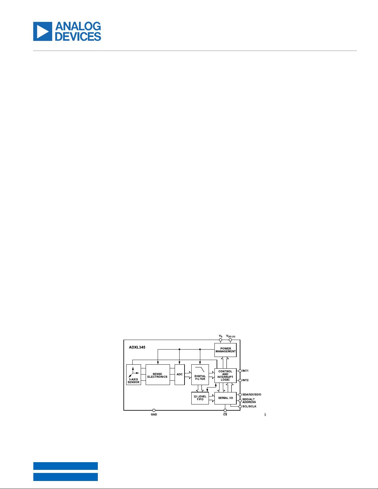
GENERAL DESCRIPTION
The ADXL345 is a small, thin, ultralow power, 3-axis accelerometer
with high resolution (13-bit) measurement at up to ±16 g. Digital
output data is formatted as 16-bit twos complement and is accessi-
ble through either a SPI (3- or 4-wire) or I
2
C digital interface.
The ADXL345 is well suited for mobile device applications. It meas-
ures the static acceleration of gravity in tilt-sensing applications, as
well as dynamic acceleration resulting from motion or shock. Its
high resolution (3.9 mg/LSB) enables measurement of inclination
changes less than 1.0°.
Several special sensing functions are provided. Activity and inactiv-
ity sensing detect the presence or lack of motion by comparing
the acceleration on any axis with user-set thresholds. Tap sensing
detects single and double taps in any direction. Free-fall sensing
detects if the device is falling. These functions can be mapped
individually to either of two interrupt output pins. An integrated
memory management system with a 32-level first in, first out (FIFO)
buffer can be used to store data to minimize host processor activity
and lower overall system power consumption.
Low power modes enable intelligent motion-based power manage-
ment with threshold sensing and active acceleration measurement
at extremely low power dissipation.
The ADXL345 is supplied in a small, thin, 3 mm × 5 mm × 1 mm,
14-lead, plastic package.
FUNCTIONAL BLOCK DIAGRAM
Figure 1.
Data Sheet ADXL345
TABLE OF CONTENTS
analog.com Rev. G | 2 of 36
Features................................................................ 1
Applications........................................................... 1
General Description...............................................1
Functional Block Diagram......................................1
Specifications........................................................ 3
Absolute Maximum Ratings...................................5
Thermal Resistance........................................... 5
Recommended Soldering Profile........................5
ESD Caution.......................................................5
Pin Configuration and Function Descriptions........ 6
Typical Performance Characteristics..................... 7
Theory of Operation.............................................12
Power Sequencing........................................... 12
Power Savings................................................. 13
Serial Communications........................................14
SPI....................................................................14
I
2
C.................................................................... 17
Interrupts............................................................. 19
DATA_READY..................................................20
SINGLE_TAP................................................... 20
DOUBLE_TAP..................................................20
Activity..............................................................20
Inactivity........................................................... 20
FREE_FALL..................................................... 20
Watermark........................................................20
Overrun............................................................ 20
FIFO.................................................................... 21
Bypass Mode....................................................21
FIFO Mode....................................................... 21
Stream Mode....................................................21
Trigger Mode.................................................... 21
Retrieving Data from FIFO............................... 21
Self-Test...............................................................22
Register Map....................................................... 23
Register Definitions.......................................... 24
Applications Information...................................... 29
Power Supply Decoupling................................ 29
Mechanical Considerations for Mounting......... 29
Tap Detection................................................... 29
Threshold......................................................... 30
Link Mode.........................................................30
Sleep Mode vs. Low Power Mode....................30
Offset Calibration..............................................30
Using Self-Test................................................. 31
Asynchronous Data Readings..........................32
Data Formatting of Upper Data Rates..............32
Noise Performance...........................................33
Operation at Voltages Other Than 2.5 V.......... 34
Offset Performance at Lowest Data Rates.......34
Axes of Acceleration Sensitivity....................... 35
Layout and Design Recommendations............ 35
Outline Dimensions............................................. 36
Ordering Guide.................................................36
Evaluation Boards............................................ 36
REVISION HISTORY
5/2022—Rev. F to Rev. G
Deleted Package Information Section..............................................................................................................5
Added Recommended Soldering Profile Section.............................................................................................5
Moved Figure 2 and Table 4............................................................................................................................ 5
Moved Table 13..............................................................................................................................................19
Change to Using Self-Test Section................................................................................................................ 31
Added Asynchronous Data Readings Section...............................................................................................32
Data Sheet ADXL345
SPECIFICATIONS
analog.com Rev. G | 3 of 36
T
A
= 25°C, V
S
= 2.5 V, V
DD I/O
= 1.8 V, acceleration = 0 g, C
S
= 10 µF tantalum, C
I/O
= 0.1 µF, output data rate (ODR) = 800 Hz, unless
otherwise noted. All minimum and maximum specifications are guaranteed. Typical specifications are not guaranteed.
Table 1.
Parameter Test Conditions Min Typ
1
Max Unit
SENSOR INPUT Each axis
Measurement Range User selectable ±2, ±4, ±8, ±16 g
Nonlinearity Percentage of full scale ±0.5 %
Inter-Axis Alignment Error ±0.1 Degrees
Cross-Axis Sensitivity
2
±1 %
OUTPUT RESOLUTION Each axis
All g Ranges 10-bit resolution 10 Bits
±2 g Range Full resolution 10 Bits
±4 g Range Full resolution 11 Bits
±8 g Range Full resolution 12 Bits
±16 g Range Full resolution 13 Bits
SENSITIVITY Each axis
Sensitivity at X
OUT
, Y
OUT
, Z
OUT
All g-ranges, full resolution 230 256 282 LSB/g
±2 g, 10-bit resolution 230 256 282 LSB/g
±4 g, 10-bit resolution 115 128 141 LSB/g
±8 g, 10-bit resolution 57 64 71 LSB/g
±16 g, 10-bit resolution 29 32 35 LSB/g
Sensitivity Deviation from Ideal All g-ranges ±1.0 %
Scale Factor at X
OUT
, Y
OUT
, Z
OUT
All g-ranges, full resolution 3.5 3.9 4.3 mg/LSB
±2 g, 10-bit resolution 3.5 3.9 4.3 mg/LSB
±4 g, 10-bit resolution 7.1 7.8 8.7 mg/LSB
±8 g, 10-bit resolution 14.1 15.6 17.5 mg/LSB
±16 g, 10-bit resolution 28.6 31.2 34.5 mg/LSB
Sensitivity Change Due to Temperature ±0.01 %/°C
0 g OFFSET Each axis
0 g Output for X
OUT
, Y
OUT
−150 0 +150 mg
0 g Output for Z
OUT
−250 0 +250 mg
0 g Output Deviation from Ideal, X
OUT
, Y
OUT
±35 mg
0 g Output Deviation from Ideal, Z
OUT
±40 mg
0 g Offset vs. Temperature for X-, Y-Axes ±0.4 mg/°C
0 g Offset vs. Temperature for Z-Axis ±1.2 mg/°C
NOISE
X-, Y-Axes 0.75 LSB rms
ODR = 100 Hz for ±2 g, 10-bit resolution or
all g-ranges, full resolution
Z-Axis 1.1 LSB rms
ODR = 100 Hz for ±2 g, 10-bit resolution or
all g-ranges, full resolution
OUTPUT DATA RATE AND BANDWIDTH User selectable
Output Data Rate (ODR)
3, 4, 5
0.1 3200 Hz
SELF-TEST
6
Output Change in X-Axis 0.20 2.10 g
Data Sheet ADXL345
SPECIFICATIONS
analog.com Rev. G | 4 of 36
Table 1.
Parameter Test Conditions Min Typ
1
Max Unit
Output Change in Y-Axis −2.10 −0.20 g
Output Change in Z-Axis 0.30 3.40 g
POWER SUPPLY
Operating Voltage Range (V
S
) 2.0 2.5 3.6 V
Interface Voltage Range (V
DD I/O
) 1.7 1.8 V
S
V
Supply Current ODR ≥ 100 Hz 140 µA
ODR < 10 Hz 30 µA
Standby Mode Leakage Current 0.1 µA
Turn-On and Wake-Up Time
7
ODR = 3200 Hz 1.4 ms
TEMPERATURE
Operating Temperature Range −40 +85 °C
WEIGHT
Device Weight 30 mg
1
The typical specifications shown are for at least 68% of the population of parts and are based on the worst case of mean ±1 σ, except for 0 g output and sensitivity, which
represents the target value. For 0 g offset and sensitivity, the deviation from the ideal describes the worst case of mean ±1 σ.
2
Cross-axis sensitivity is defined as coupling between any two axes.
3
Bandwidth is the −3 dB frequency and is half the output data rate, bandwidth = ODR/2.
4
The output format for the 3200 Hz and 1600 Hz ODRs is different than the output format for the remaining ODRs. This difference is described in the Data Formatting of
Upper Data Rates section.
5
Output data rates below 6.25 Hz exhibit additional offset shift with increased temperature, depending on selected output data rate. Refer to the Offset Performance at
Lowest Data Rates section for details.
6
Self-test change is defined as the output (g) when the SELF_TEST bit = 1 (in the DATA_FORMAT register, Address 0x31) minus the output (g) when the SELF_TEST bit
= 0. Due to device filtering, the output reaches its final value after 4 × τ when enabling or disabling self-test, where τ = 1/(data rate). The part must be in normal power
operation (LOW_POWER bit = 0 in the BW_RATE register, Address 0x2C) for self-test to operate correctly.
7
Turn-on and wake-up times are determined by the user-defined bandwidth. At a 100 Hz data rate, the turn-on and wake-up times are each approximately 11.1 ms. For other
data rates, the turn-on and wake-up times are each approximately τ + 1.1 in milliseconds, where τ = 1/(data rate).
Data Sheet ADXL345
ABSOLUTE MAXIMUM RATINGS
analog.com Rev. G | 5 of 36
Table 2.
Parameter Rating
Acceleration
Any Axis, Unpowered 10,000 g
Any Axis, Powered 10,000 g
V
S
−0.3 V to +3.9 V
V
DD I/O
−0.3 V to +3.9 V
Digital Pins −0.3 V to V
DD I/O
+ 0.3 V or 3.9 V,
whichever is less
All Other Pins −0.3 V to +3.9 V
Output Short-Circuit Duration (Any Pin
to Ground)
Indefinite
Temperature Range
Powered −40°C to +105°C
Storage −40°C to +105°C
Stresses at or above those listed under Absolute Maximum Ratings
may cause permanent damage to the product. This is a stress
rating only; functional operation of the product at these or any other
conditions above those indicated in the operational section of this
specification is not implied. Operation beyond the maximum operat-
ing conditions for extended periods may affect product reliability.
THERMAL RESISTANCE
Table 3. Package Characteristics
Package Type θ
JA
θ
JC
Device Weight
14-Terminal LGA 150°C/W 85°C/W 30 mg
RECOMMENDED SOLDERING PROFILE
Figure 2 and Table 4 provide details about the recommended
soldering profile.
Figure 2. Recommended Soldering Profile
Table 4. Recommended Soldering Profile
1, 2
Profile Feature
Condition
Sn63/Pb37 Pb-Free
Average Ramp Rate from Liquid Temperature
(T
L
) to Peak Temperature (T
P
)
3°C/sec max-
imum
3°C/sec maxi-
mum
Preheat
Minimum Temperature (T
SMIN
) 100°C 150°C
Maximum Temperature (T
SMAX
) 150°C 200°C
Time from T
SMIN
to T
SMAX
(t
S
) 60 sec to 120
sec
60 sec to 180
sec
T
SMAX
to T
L
Ramp-Up Rate 3°C/sec max-
imum
3°C/sec maxi-
mum
Liquid Temperature (T
L
) 183°C 217°C
Time Maintained Above T
L
(t
L
) 60 sec to 150
sec
60 sec to 150
sec
Peak Temperature (T
P
) 240 + 0/−5°C 260 + 0/−5°C
Time of Actual T
P
− 5°C (t
P
) 10 sec to 30
sec
20 sec to 40
sec
Ramp-Down Rate 6°C/sec max-
imum
6°C/sec maxi-
mum
Time 25°C to Peak Temperature 6 minutes
maximum
8 minutes
maximum
1
Based on JEDEC Standard J-STD-020D.1.
2
For best results, the soldering profile should be in accordance with the recom-
mendations of the manufacturer of the solder paste used.
ESD CAUTION
ESD (electrostatic discharge) sensitive device. Charged devi-
ces and circuit boards can discharge without detection. Although
this product features patented or proprietary protection circuitry,
damage may occur on devices subjected to high energy ESD.
Therefore, proper ESD precautions should be taken to avoid
performance degradation or loss of functionality.
剩余35页未读,继续阅读
资源评论
2201_75698556
- 粉丝: 6
- 资源: 4
上传资源 快速赚钱
- 我的内容管理 展开
- 我的资源 快来上传第一个资源
- 我的收益 登录查看自己的收益
- 我的积分 登录查看自己的积分
- 我的C币 登录后查看C币余额
- 我的收藏
- 我的下载
- 下载帮助
最新资源
- 937712277954201实习5.word
- 2程序语言基础知识pdf1_1716337722703.jpeg
- 简单的Python示例,演示了如何使用TCP/IP协议进行基本的客户端和服务器通信
- 考试.sql
- keil2 + proteus + 8051.exe
- 1961ee27df03bd4595d28e24b00dde4e_744c805f7e4fb4d40fa3f695bfbab035_8(1).c
- mediapipe-0.9.0.1-cp37-cp37m-win-amd64.whl.zip
- windows注册表编辑工具
- mediapipe-0.9.0.1-cp37-cp37m-win-amd64.whl.zip
- 校园通行码预约管理系统20240522075502
资源上传下载、课程学习等过程中有任何疑问或建议,欢迎提出宝贵意见哦~我们会及时处理!
点击此处反馈
安全验证
文档复制为VIP权益,开通VIP直接复制
信息提交成功