


Copyright © Lattice Semiconductor 2006
Sept 2006 Lattice Software Training
Bringing the Best TogetherBringing the Best Together
Lattice Confidential
How to design FSM
Lattice Semiconductor
Westor Wang ATM
Copyright © Lattice Semiconductor 2006
Sept 2006 Lattice Software Training
Bringing the Best TogetherBringing the Best Together
Lattice Confidential
Logic Density (System Gates)
GH
O
Lattice Low Cost FPGA solutions
2004
ORCA4 (FPSC)
150nm SRAM
5K –16K LUT
4.25Gbps SERDES
XPGA
180nm Embedded E2
2K –15K LUT
850Mbps SERDES
Low Cost
Solutions
GHO
2005
TBA
EC
0.13um SRAM
1.5K –41K LUT
750Mbps I/O
Low Cost
SC
90nm SRAM
15K-80K LUT
8-32 SERDES
High
Performance
Solutions
ECP
130nm SRAM
6.1K –33K LUT
750Mbps I/O + DSP
Cost Effective DSP
SC - II
65/90nm SRAM
ECP - II
90nm SRAM
XP II
90nm Embedded Flash
XO
130nm Embedded Flash
256 –2280 LUTs
Extreme Low Cost
XP
130nm Embedded Flash
3K –20K LUTs
Low Cost
Low Cost Non-Volatile Instant On FPGA Offering
Low Cost SRAM-based FPGA Offering
High Performance SERDES SRAM-based FPGA Offering
Copyright © Lattice Semiconductor 2006
Sept 2006 Lattice Software Training
Bringing the Best TogetherBringing the Best Together
Lattice Confidential
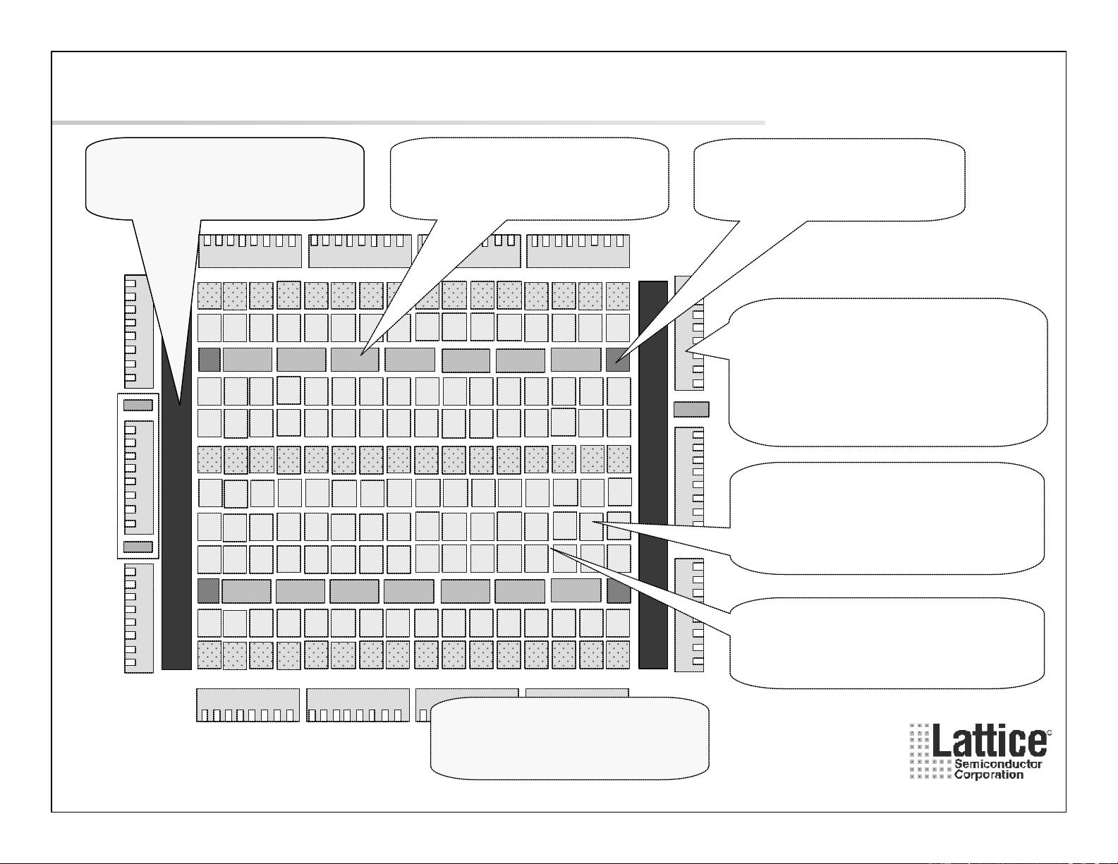
ispXP FLASH Memory
Instant-on, Secure and
Single-chip
LatticeXP: Added Non-Volatility
JTAG
sysMEM
TM
Block RAM
9kbit Dual Port
Optimized sysIO
TM
Buffers
Support Mainstream I/O;
LVCMOS/LVTTL, LVDS,
SSTL, HSTL,DDR Memory
Interfaces
sysCLOCK
TM
PLLs
Frequency Synthesis &
Clock Alignment
Optimized Programmable
Function Units (PFUs)
25% –Logic + RAM
75% –Logic Only
Flexible Routing
Optimized for Speed, Cost
and Routability
No sysDSP Option
Copyright © Lattice Semiconductor 2006
Sept 2006 Lattice Software Training
Bringing the Best TogetherBringing the Best Together
Lattice Confidential
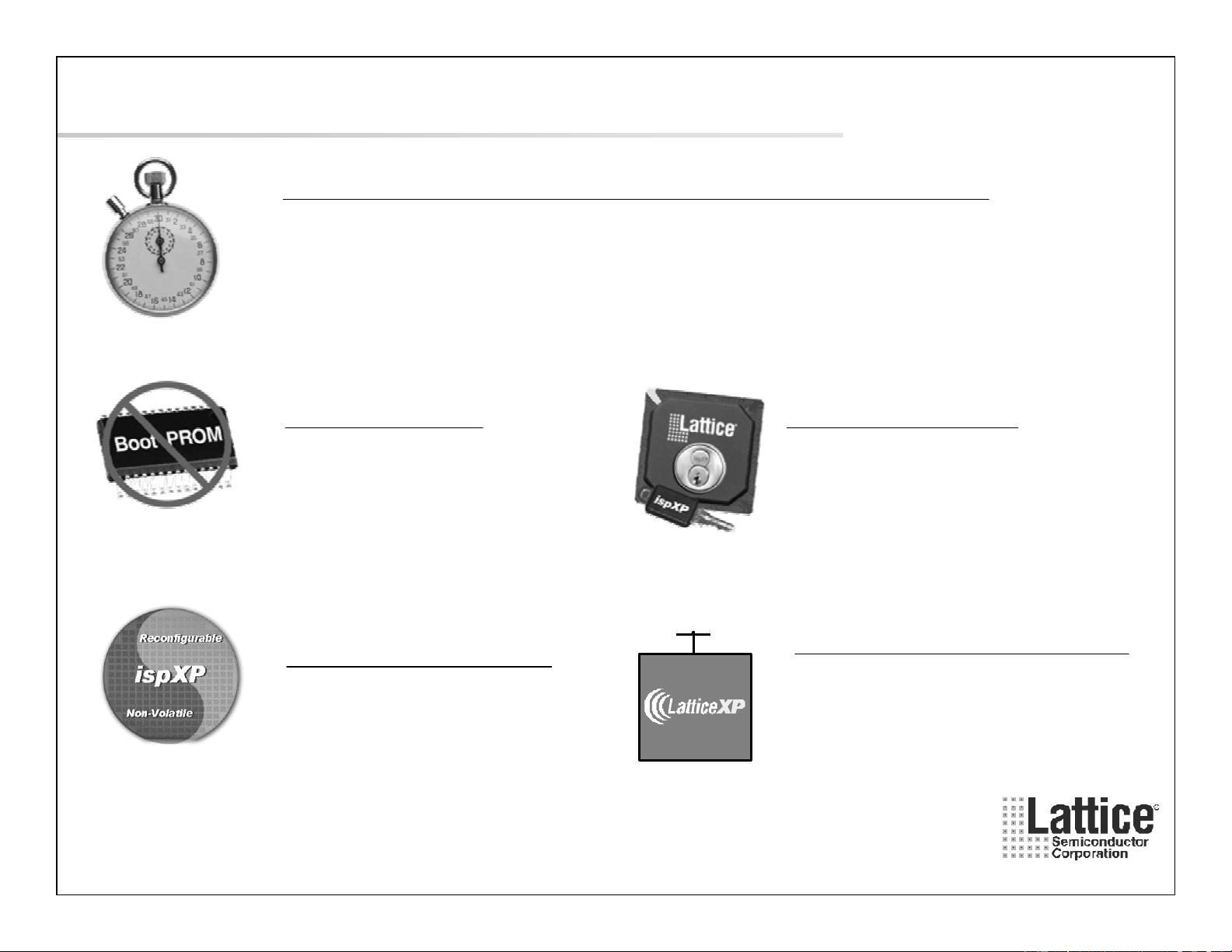
LatticeXP Benefits
Self-Configuration in Under A Millisecond
•Ideal for system “heartbeat”control logic
•Supports configuration “scrubbing”for SEU control
•Supports rapid power cycling
High Security
•Security bits prevent readback
•No exposed power-up bitstream
Single Chip
•Simplify design
•Reduced PCB footprint
•Save boot PROM costs
SRAM + FLASH
•TransFR (TFR) technology
enables in field updates
while system operates
On-Chip Regulation
•Support legacy applications
with latest technology
- Reduce costs
- Improve performance
3.3, 2.5, 1.8
or 1.2V
3.3, 2.5, 1.8
or 1.2V
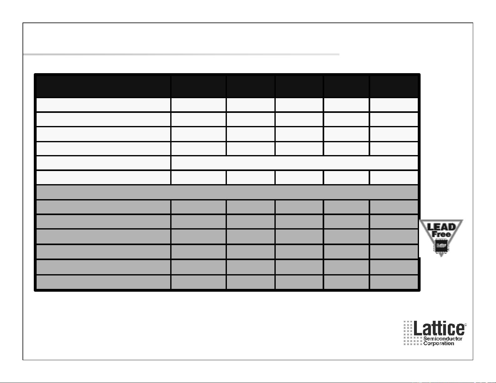
Copyright © Lattice Semiconductor 2006
Sept 2006 Lattice Software Training
Bringing the Best TogetherBringing the Best Together
Lattice Confidential
LatticeXP Family
62100-pin TQFP (14x14mm)
340300484-ball fpBGA (23x23mm)
268268244388-ball fpBGA (23x23mm)
188188188188256-ball fpBGA (17x17mm)
142136208-pin PQFP (28x28mm)
100100144-pin TQFP (20x20mm)
Package I/O Combinations
44422PLLs
1.2/1.8/2.5/3.3VVoltage (V)
7961392312Distributed RAM (Kbits)
4142882169054sysMEM (Kbits)
463224106sysMEM Blocks
19.715.49.75.83.1LUTs (K)
XP20XP15XP10XP6XP3Device
RoHS


