PIC16F18323数据手册


2015 Microchip Technology Inc. Preliminary DS40001799A-page 1
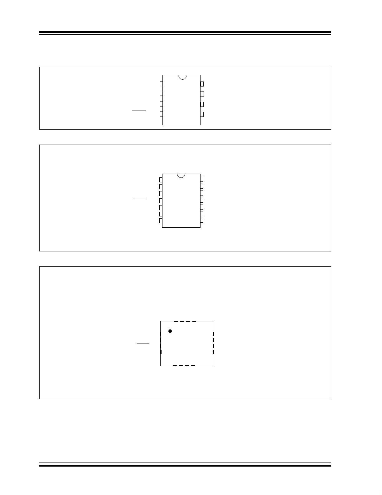
PIC16(L)F18313/18323
Description
PIC16(L)F18313/18323 microcontrollers feature Analog, Core Independent Peripherals and Communication
Peripherals, combined with eXtreme Low Power (XLP) for wide range of general purpose and low-power applications.
The Peripheral Pin Select (PPS) functionality enables pin mapping when using the digital peripherals (CLC, CWG,
CCP, PWM and communications) to add flexibility to the application design.
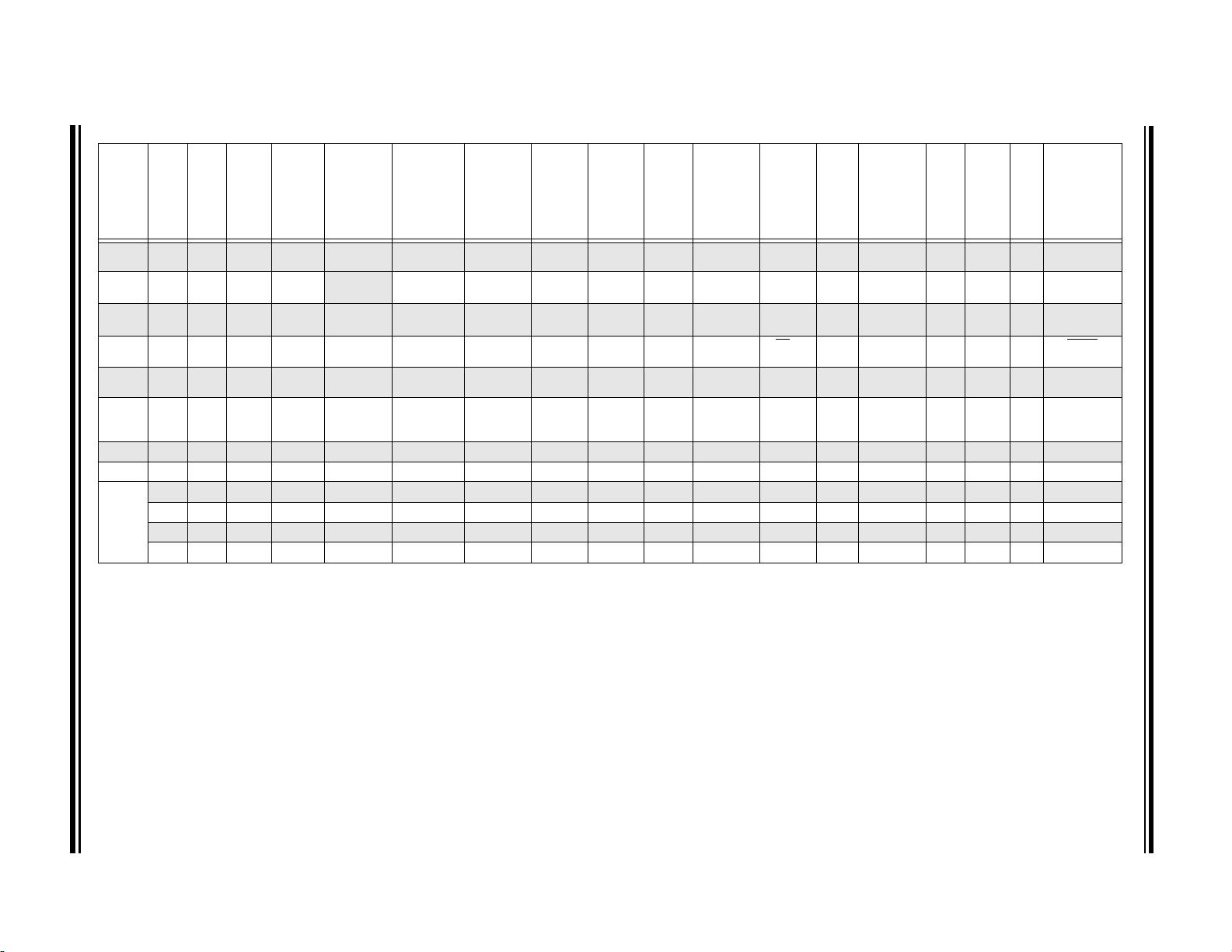
Core Features
• C Compiler Optimized RISC Architecture
• Only 49 Instructions
• Operating Speed:
- DC – 32 MHz clock input
- 125 ns minimum instruction cycle
• Interrupt Capability
• 16-Level Deep Hardware Stack
• Two 8-bit Timers
• One 16-bit Timer
• Low-Current Power-on Reset (POR)
• Configurable Power-up Timer (PWRTE)
• Brown-out Reset (BOR) with Fast Recovery
• Low-Power BOR (LPBOR) Option
• Extended Watchdog Timer (WDT) with Dedicated
On-chip Oscillator for Reliable Operation
• Programmable Code Protection
Memory
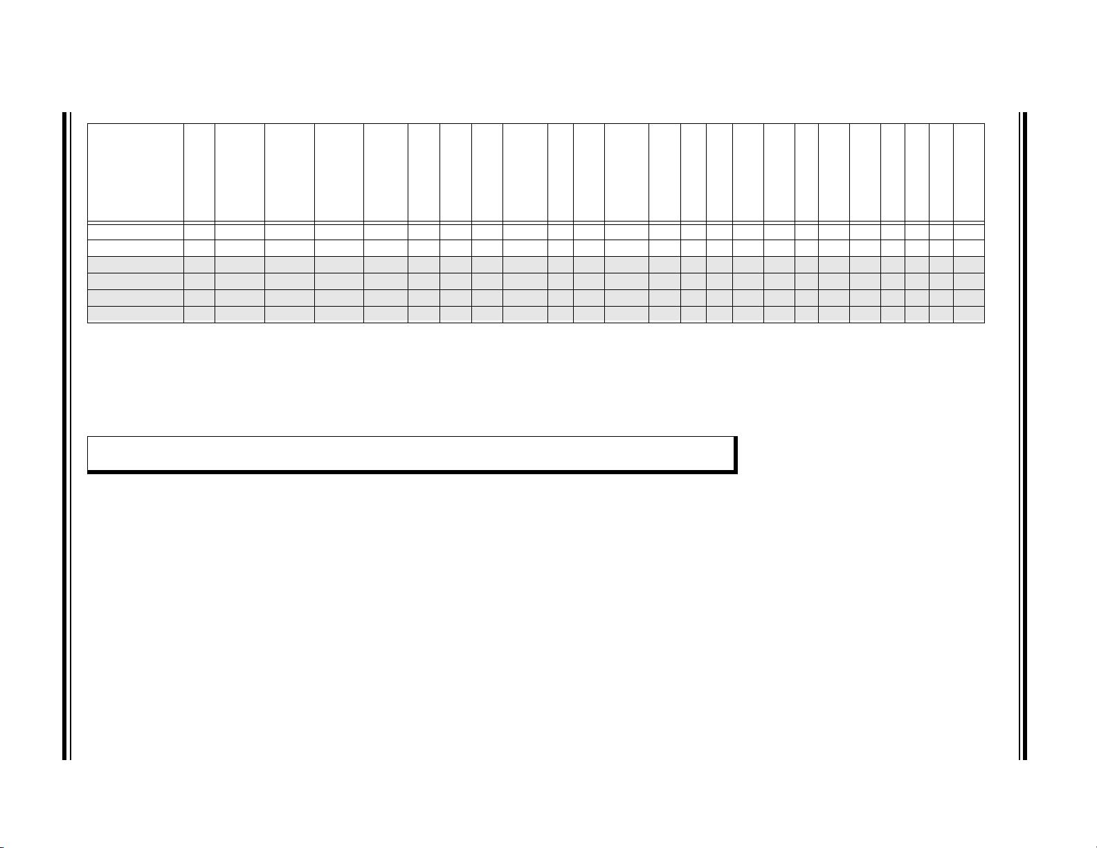
• 3.5 KB Flash Program Memory
• 256B Data SRAM Memory
• 256B of EEPROM
• Direct, Indirect and Relative Addressing Modes
Operating Characteristics
• Operating Voltage Range:
- 1.8V to 3.6V (PIC16LF18313/18323)
- 2.3V to 5.5V (PIC16F18313/18323)
• Temperature Range:
- Industrial: -40°C to 85°C
- Extended: -40°C to 125°C
eXtreme Low-Power (XLP) Features
• Sleep mode: 40 nA @ 1.8V, typical
• Watchdog Timer: 250 nA @ 1.8V, typical
• Secondary Oscillator: 300 nA @ 32 kHz
• Operating Current:
- 8 uA @ 32 kHz, 1.8V, typical
- 37 uA/MHz @ 1.8V, typical
Power-Saving Operating Modes
• IDLE: Ability to put the CPU core to Sleep while
internal peripherals continue operating from the
system clock
• DOZE: Ability to run the CPU core slower than the
system clock used by the internal peripherals
• SLEEP: Lowest Power Consumption
• Peripheral Module Disable (PMD): Peripheral
power disable hardware module to minimize
power consumption of unused peripherals
Digital Peripherals
• Configurable Logic Cell (CLC):
- Two CLCs
- Integrated combinational and sequential logic
• Complementary Waveform Generator (CWG):
- Rising and falling edge dead-band control
- Full-bridge, half-bridge, 1-channel drive
- Multiple signal sources
• Capture/Compare/PWM (CCP) modules:
- Two CCPs
- 16-bit resolution for Capture/Compare modes
- 10-bit resolution for PWM mode
• Pulse-Width Modulators:
-Two 10-bit PWMs
• Numerically Controlled Oscillator (NCO):
- Precision linear frequency generator(@50%
duty cycle) with 0.0001% step size of source
input clock
- Input Clock: 0 Hz < F
NCO
< 32 MHz
- Resolution: F
NCO
/2
20
• Serial Communications:
- EUSART
- RS-232, RS-485, LIN compatible
- Auto-baud detect, Auto-wake-up on start
- Master Synchronous Serial Port (MSSP)
- SPI
-I
2
C™, SMBus, PMBus™ compatible
• Data Signal Modulator (DSM):
- Modulates a carrier signal with digital data to
create custom carrier synchronized output
waveforms
Full-Featured, Low Pin Count Microcontrollers with XLP

剩余441页未读,继续阅读
资源评论

 uestc_somnus2018-07-07很好的资源,多谢分享
- starling882016-07-07不错,只是有一点可惜的是,它是英文的。


