没有合适的资源?快使用搜索试试~ 我知道了~
DAC0802中文资料
需积分: 10 14 下载量 35 浏览量
2009-07-29
18:15:11
上传
评论
收藏 346KB PDF 举报
温馨提示
试读
11页
~~~~~~~~~~~~~~~~~~~~~~~~~~~~~~~~~~~~~~~~~~~~
资源推荐
资源详情
资源评论
DAC0800/DAC0802
8-Bit Digital-to-Analog Converters
General Description
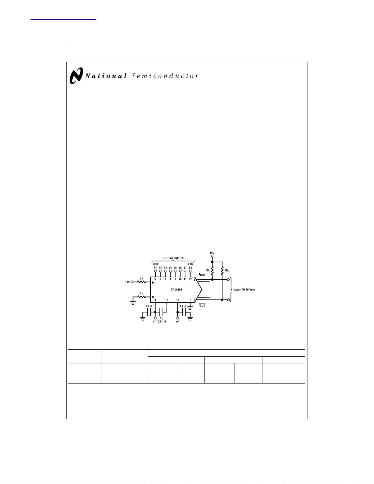
The DAC0800 series are monolithic 8-bit high-speed
current-output digital-to-analog converters (DAC) featuring
typical settling times of 100 ns. When used as a multiplying
DAC, monotonic performance over a 40 to 1 reference cur-
rent range is possible. The DAC0800 series also features
high compliance complementary current outputs to allow dif-
ferential output voltages of 20 Vp-p with simple resistor loads
as shown in
Figure 1
. The reference-to-full-scale current
matching of better than
±
1 LSB eliminates the need for
full-scale trims in most applications while the nonlinearities
of better than
±
0.1
%
over temperature minimizes system er-
ror accumulations.
The noise immune inputs of the DAC0800 series will accept
TTL levels with the logic threshold pin, V
LC
, grounded.
Changing the V
LC
potential will allow direct interface to other
logic families. The performance and characteristics of the
device are essentially unchanged over the full
±
4.5V to
±
18V power supply range; power dissipation is only 33 mW
with
±
5V supplies and is independent of the logic input
states.
The DAC0800, DAC0802, DAC0800C and DAC0802C are a
direct replacement for the DAC-08, DAC-08A, DAC-08C,
and DAC-08H, respectively.
Features
n Fast settling output current: 100 ns
n Full scale error:
±
1 LSB
n Nonlinearity over temperature:
±
0.1
%
n Full scale current drift:
±
10 ppm/˚C
n High output compliance: −10V to +18V
n Complementary current outputs
n Interface directly with TTL, CMOS, PMOS and others
n 2 quadrant wide range multiplying capability
n Wide power supply range:
±
4.5V to
±
18V
n Low power consumption: 33 mW at
±
5V
n Low cost
Typical Applications
Ordering Information
Non-Linearity Temperature Order Numbers
Range J Package (J16A) (Note 1) N Package (N16E) (Note 1) SO Package (M16A)
±
0.1
%
FS 0˚C ≤ T
A
≤ +70˚C DAC0802LCJ DAC-08HQ DAC0802LCN DAC-08HP DAC0802LCM
±
0.19
%
FS −55˚C ≤ T
A
≤ +125˚C DAC0800LJ DAC-08Q
±
0.19
%
FS 0˚C ≤ T
A
≤ +70˚C DAC0800LCJ DAC-08EQ DAC0800LCN DAC-08EP DAC0800LCM
Note 1: Devices may be ordered by using either order number.
DS005686-1
FIGURE 1.
±
20 V
P-P
Output Digital-to-Analog Converter (Note 5)
June 1999
DAC0800/DAC0802 8-Bit Digital-to-Analog Converters
© 1999 National Semiconductor Corporation DS005686 www.national.com
查询DAC0800供应商
Absolute Maximum Ratings (Note 2)
If Military/Aerospace specified devices are required,
please contact the National Semiconductor Sales Office/
Distributors for availability and specifications.
Supply Voltage (V
+
−V
−
)
±
18V or 36V
Power Dissipation (Note 3) 500 mW
Reference Input Differential Voltage
(V14 to V15) V
−
to V
+
Reference Input Common-Mode
Range (V14, V15) V
−
to V
+
Reference Input Current 5 mA
Logic Inputs V
−
to V
−
plus 36V
Analog Current Outputs
(V
S
−
=
−15V) 4.25 mA
ESD Susceptibility (Note 4) TBD V
Storage Temperature −65˚C to +150˚C
Lead Temp. (Soldering, 10 seconds)
Dual-In-Line Package (plastic) 260˚C
Dual-In-Line Package (ceramic) 300˚C
Surface Mount Package
Vapor Phase (60 seconds) 215˚C
Infrared (15 seconds) 220˚C
Operating Conditions (Note 2)
Min Max Units
Temperature (T
A
)
DAC0800L −55 +125 ˚C
DAC0800LC 0 +70 ˚C
DAC0802LC 0 +70 ˚C
Electrical Characteristics
The following specifications apply for V
S
=
±
15V, I
REF
=
2 mA and T
MIN
≤ T
A
≤ T
MAX
unless otherwise specified. Output
characteristics refer to both I
OUT
and I
OUT
.
DAC0802LC DAC0800L/
Symbol Parameter Conditions DAC0800LC Units
Min Typ Max Min Typ Max
Resolution 888888Bits
Monotonicity 888888Bits
Nonlinearity
±
0.1
±
0.19
%
FS
t
s
Settling Time To
±
1
⁄
2
LSB, All Bits Switched 100 135 ns
“ON” or “OFF”, T
A
=
25˚C
DAC0800L 100 135 ns
DAC0800LC 100 150 ns
tPLH, Propagation Delay T
A
=
25˚C
tPHL Each Bit 35 60 35 60 ns
All Bits Switched 35 60 35 60 ns
TCI
FS
Full Scale Tempco
±
10
±
50
±
10
±
50 ppm/˚C
V
OC
Output Voltage Compliance Full Scale Current Change −10 18 −10 18 V
<
1
⁄
2
LSB, R
OUT
>
20 MΩ Typ
I
FS4
Full Scale Current V
REF
=
10.000V, R14
=
5.000 kΩ 1.984 1.992 2.000 1.94 1.99 2.04 mA
R15
=
5.000 kΩ,T
A
=
25˚C
I
FSS
Full Scale Symmetry I
FS4
−I
FS2
±
0.5
±
4.0
±
1
±
8.0 µA
I
ZS
Zero Scale Current 0.1 1.0 0.2 2.0 µA
I
FSR
Output Current Range V
−
=
−5V 0 2.0 2.1 0 2.0 2.1 mA
V
−
=
−8V to −18V 0 2.0 4.2 0 2.0 4.2 mA
Logic Input Levels
V
IL
Logic “0” V
LC
=
0V 0.8 0.8 V
V
IH
Logic “1” 2.0 2.0 V
Logic Input Current V
LC
=
0V
I
IL
Logic “0” −10V≤V
IN
≤+0.8V −2.0 −10 −2.0 −10 µA
I
IH
Logic “1” 2V≤V
IN
≤+18V 0.002 10 0.002 10 µA
V
IS
Logic Input Swing V
−
=
−15V −10 18 −10 18 V
V
THR
Logic Threshold Range V
S
=
±
15V −10 13.5 −10 13.5 V
I
15
Reference Bias Current −1.0 −3.0 −1.0 −3.0 µA
dl/dt Reference Input Slew Rate (
Figure 11
) 4.0 8.0 4.0 8.0 mA/µs
PSSI
FS+
Power Supply Sensitivity 4.5V≤V
+
≤18V 0.0001 0.01 0.0001 0.01
%
/
%
PSSI
FS−
−4.5V≤V
−
≤18V 0.0001 0.01 0.0001 0.01
%
/
%
I
REF
=
1mA
www.national.com 2
Electrical Characteristics (Continued)
The following specifications apply for V
S
=
±
15V, I
REF
=
2 mA and T
MIN
≤ T
A
≤ T
MAX
unless otherwise specified. Output
characteristics refer to both I
OUT
and I
OUT
.
DAC0802LC DAC0800L/
Symbol Parameter Conditions DAC0800LC Units
Min Typ Max Min Typ Max
Power Supply Current V
S
=
±
5V, I
REF
=
1mA
I+ 2.3 3.8 2.3 3.8 mA
I− −4.3 −5.8 −4.3 −5.8 mA
V
S
=
5V, −15V, I
REF
=
2mA
I+ 2.4 3.8 2.4 3.8 mA
I− −6.4 −7.8 −6.4 −7.8 mA
V
S
=
±
15V, I
REF
=
2mA
I+ 2.5 3.8 2.5 3.8 mA
I− −6.5 −7.8 −6.5 −7.8 mA
P
D
Power Dissipation
±
5V, I
REF
=
1mA 3348 3348mW
5V,−15V, I
REF
=
2 mA 108 136 108 136 mW
±
15V, I
REF
=
2 mA 135 174 135 174 mW
Note 2: Absolute Maximum Ratings indicate limits beyond which damage to the device may occur. DC and AC electrical specifications do not apply when operating
the device beyond its specified operating conditions.
Note 3: The maximum junction temperature of the DAC0800 and DAC0802 is 125˚C. For operating at elevated temperatures, devices in the Dual-In-Line J package
must be derated based on a thermal resistance of 100˚C/W, junction-to-ambient, 175˚C/W for the molded Dual-In-Line N package and 100˚C/W for the Small Outline
M package.
Note 4: Human body model, 100 pF discharged through a 1.5 kΩ resistor.
Note 5: Pin-out numbers for the DAC080X represent the Dual-In-Line package. The Small Outline package pin-out differs from the Dual-In-Line package.
Connection Diagrams
Dual-In-Line Package
DS005686-13
Top View
Small Outline Package
DS005686-14
Top View
See Ordering Information
www.national.com3
剩余10页未读,继续阅读
资源评论
qq10800277
- 粉丝: 0
- 资源: 3
上传资源 快速赚钱
- 我的内容管理 展开
- 我的资源 快来上传第一个资源
- 我的收益 登录查看自己的收益
- 我的积分 登录查看自己的积分
- 我的C币 登录后查看C币余额
- 我的收藏
- 我的下载
- 下载帮助
安全验证
文档复制为VIP权益,开通VIP直接复制
信息提交成功