


Rev. 1 – June 2013
@2013 Semtech Corporation 1 of 13 www.semtech.com
SX1232 LNA and PA Impedance Matching
Techniques
AN1200.16
Application Note:
SX1232 LNA and PA Impedance Matching
Techniques

Rev. 1 – June 2013
@2013 Semtech Corporation 2 of 13 www.semtech.com
SX1232 LNA and PA Impedance Matching
Techniques
1 Table of Contents
1 Table of Contents .......................................................................................................................... 2
1.1 Index of Figures .................................................................................................................... 2
1.2 Index of Tables ..................................................................................................................... 2
2 Introduction ................................................................................................................................... 3
3 General Impedance Matching Theory ........................................................................................... 3
4 SX1232 Impedance Matching ....................................................................................................... 3
4.1 LNA Impedance Matching, split path case ............................................................................ 3
4.1.1 Test Setup for sensitivity measurement ............................................................................ 3
4.1.2 Measurement of RFI optimum source impedance ............................................................. 4
4.1.3 Measurement of 1dB noise impedance circles .................................................................. 5
4.1.4 Designing the matching network ....................................................................................... 6
4.2 LNA Impedance Matching, combined RFI and RFO ports .................................................... 7
4.3 Power Amplifier Impedance Matching RFO port ................................................................... 7
4.3.1 Standard Matching Network, RFO Port ............................................................................. 9
4.4 Power Amplifier Matching, PA_BOOST Port ....................................................................... 11
4.5 Separate RFO and RFI Ports .............................................................................................. 12
1.1 Index of Figures
Figure 1 RFI Input Match Test Setup .................................................................................................... 4
Figure 2 LNA Source Impedance Measurement Setup ........................................................................ 4
Figure 3: Smith Chart Plot of Optimum Noise Match and 1 dB Circle ................................................... 5
Figure 4 Smith Chart showing plot of matching components ............................................................... 6
Figure 5 Input matching circuit schematic, ............................................................................................ 6
Figure 6 Input matching with combined RFI and RFO ports ................................................................. 7
Figure 7 Power Amplifier Load Impedance Measurement Setup .......................................................... 8
Figure 8 PA Load Pull Results .............................................................................................................. 8
Figure 9 Three Step Matching ............................................................................................................ 10
Figure 10 PA_BOOST Matching Network ........................................................................................... 11
Figure 11 Combined Network for Separate RFO and RFI Ports ........................................................ 12
1.2 Index of Tables
Table 1 RFI Optimum and 1dB source impedance values .................................................................... 5
Table 2 Tabulated Load Pull Results .................................................................................................... 9
Table 3 RFO Port Performance .......................................................................................................... 11

Rev. 1 – June 2013
@2013 Semtech Corporation 3 of 13 www.semtech.com
SX1232 LNA and PA Impedance Matching
Techniques
2 Introduction
The purpose of this technical note is to assist the engineer in understanding the techniques necessary
for proper impedance matching of the LNA and PA ports of the SX1232. Included in this discussion
are methods for optimizing receiver sensitivity by providing the optimum impedance transformation
from a 50 Ohm source to the SX1232 RFI port. In addition, a similar discussion will describe
techniques for providing the optimum load impedance for both the RFO and PA_BOOST ports, which
will simultaneously provide maximum power, minimum current, and reduced harmonic content.
Minimizing harmonic content by proper matching is important because it will simplify the additional
filtering necessary to meet regulatory requirements for harmonic and spurious radiation.
The three ports provided on the SX1232, the RFI, RFO, and PA_BOOST can be used independently
by connecting to a T/R switch. Alternatively, the RFI and RFO can be connected together using
passive components to provide a transmit/receive port. Configuring these ports will also be
discussed.
3 General Impedance Matching Theory
In practice, impedance matching involves designing a circuit which transfers power efficiently from
one impedance to another. In most cases, one of the impedances is a known 50 Ohm resistive load
while the other can be a combination of a higher or lower resistive component along with a reactive
component. Maximum power transfer is achieved when the resistive component of the source is
identical to that of the load while the reactance of the load is cancelled by the source. So the problem
becomes one of developing a network which simultaneously transforms the source impedance to the
load while cancelling out the reactive components. The conventional approach would be to measure
the unknown impedance using a vector network analyzer (VNA) or other impedance measuring
device. Then using analytic techniques (Smith Chart or computer simulation), develop the network
that provides the required matching function. For the case of both LNA and Power Amplifier
impedance matching however, simply measuring the device impedance and matching that impedance
to the desired 50 Ohm load will not yield the best performance. In order to achieve the optimum
source impedance for the LNA and load impedance for the PA, a technique referred to as “load pull”
is generally used. This involves using an adjustable tuner which can provide a continuously variable
impedance match from a 50 Ohm port to the LNA or PA port allowing independent adjustment of both
the resistive and reactive components. The tuner is adjusted while monitoring critical performance
parameters (receiver sensitivity, power output, current drain, harmonic content etc) until an optimum
level of performance is achieved. Then the impedance of this tuner input is measured and that
becomes the optimum LNA source or PA load impedance. A network is then developed that
transforms 50 Ohms to this value.
4 SX1232 Impedance Matching
4.1 LNA Impedance Matching, split path case
The following tutorial will illustrate how to measure optimum LNA noise match impedance and how to
create a 50 Ohm impedance matching network for the case where the RFI port is connected to a T/R
switch or Front End Module. In 4.2, we will discuss the case where the RFI and RFO ports are
combined into a single antenna port.
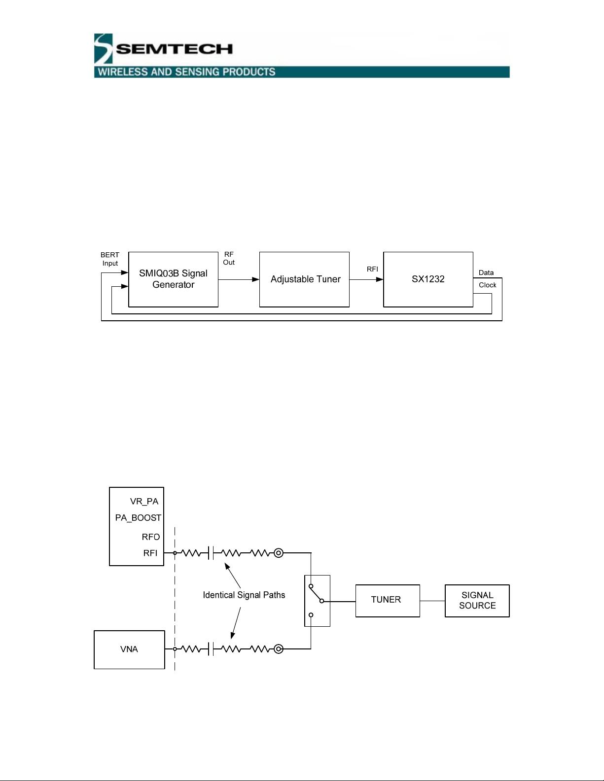
4.1.1 Test Setup for sensitivity measurement
As discussed earlier, the optimum impedance match for the SX1232 RFI port involves the use of an
adjustable tuner to vary the source impedance while monitoring performance, in this case receive
sensitivity. A simplified block diagram of the test setup is shown in Figure 1. An R/S SMIQ03B signal
generator with BERT option is used in this application, but any equivalent generator with bit error rate
test capability can be used. An FSK modulated pseudo-random data pattern is used to provide the
input test signal for the SX1232. This signal amplitude is varied by the R/S SMIQ03B output level
Rev. 1 – June 2013
@2013 Semtech Corporation 4 of 13 www.semtech.com
SX1232 LNA and PA Impedance Matching
Techniques
control. This FSK modulated signal is connected to the SX1232 RFI port through the adjustable
tuner. The characteristics of this modulated signal are not important, as long as the SX1232 is
properly configured to demodulate it and delivers it with recovered clock back to the R/S SMIQ. The
BERT function compares this demodulated data with what was originally sent. This way, bit errors
and hence bit error rate (BER) can be measured and observed in real time. By simultaneously
reducing the signal level, and adjusting the tuner for minimum BER and further reducing the signal
level, an iterative process is used to find the minimum signal level for a given BER (0.1% in this case).
The optimum source impedance is achieved when no further improvement by tuning can be
measured. When this tuner setting has been reached, the tuner is disconnected from the RFI input
and its impedance is measured. It is recommended that this test be performed in a shielded room or
to place the SX1232 in a shielded enclosure so that interfering signals will not impact the sensitivity
measurement.
Figure 1 RFI Input Match Test Setup
4.1.2 Measurement of RFI optimum source impedance
Once the tuner has been adjusted for minimum signal level (or best sensitivity) the source impedance
driving the RFI port is measured. If an automatic tuner is used, then a measurement setup as shown
in Figure 2 can be used. Two identical signal paths are established (same cable length, connectors,
etc.) so that this impedance can be easily measured by simply throwing a switch. Thus the tuner
impedance presented at the RFI port can also be presented directly to the calibration plane of the
VNA for accurate measurement. Or use a manual tuner and RF switch. The tuner can be automated
or manual (refer to AN1200.04).
Calibration Plane
Figure 2 LNA Source Impedance Measurement Setup


