没有合适的资源?快使用搜索试试~ 我知道了~
AT88SC0104C Datasheet
5星 · 超过95%的资源 需积分: 10 9 下载量 186 浏览量
2013-06-14
02:39:18
上传
评论
收藏 208KB PDF 举报
温馨提示
试读
20页
AT88SCxx系列加密存储芯片是国际着名芯片厂商Atmel公司生产的具备多用途的加密存储系列芯片。其中AT88SC1616是该系列芯片的典型代表。由于其具备多达2KB的EEPROM,利用I2C串行总线通信,采用认证或加密验证等方式进行数据访问,因此以其容量大、体积小、使用方便、安全可靠等特点,在产生研发中得到了广泛的应用。 内部结构 高安全性。对于用户民应用区,具备标准访问、认证访问和加密验证访问两种方式,同时提供多组密码集供读写访问使用。每个应用分区在配置区中都有相应的寄存器控制其安全等级和访问方式。
资源推荐
资源详情
资源评论
•
Atmel AT88SC0104C
Atmel CryptoMemory, 1Kbit
SUMMARY DATASHEET
Features
• One of a family of nine devices with user memories from 1Kbit to 256Kbit
• 1Kbit (128-byte) EEPROM user memory
• Four 32 byte (256 bit) zones
• Self-timed write cycle
• Single byte or 16-byte page write mode
• Programmable access rights for each zone
• 2Kbit configuration zone
• 37-byte OTP area for user-defined codes
• 160-byte area for user-defined keys and passwords
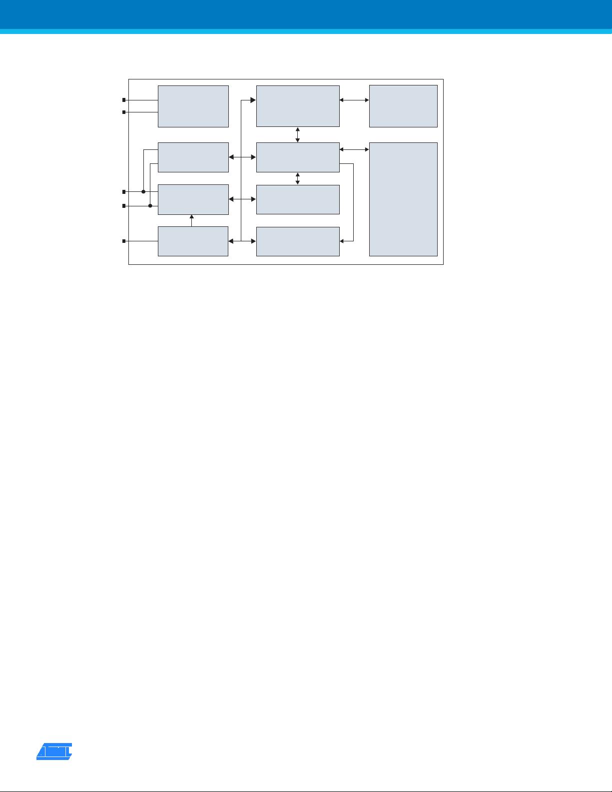
• High security features
• 64-bit mutual authentication protocol (under license of ELVA)
• Encrypted checksum
• Stream encryption
• Four key sets for authentication and encryption
• Eight sets of two 24-bit passwords
• Anti-tearing function
• Voltage and frequency monitor
• Smart card features
• ISO 7816 Class A (5V) or Class B (3V) operation
• ISO 7816-3 asynchronous T = 0 protocol (Gemplus
®
patent) *
• Multiple zones, key sets and passwords for multi-application use
• Synchronous two-wire serial interface for faster device initialization *
• Programmable 8-byte answer-to-reset register
• ISO 7816-2 compliant modules
• Embedded application features
• Low voltage operation: 2.7V to 5.5V
• Secure nonvolatile storage for sensitive system or user information
• Two-wire serial interface
• 1.0MHz compatibility for fast operation
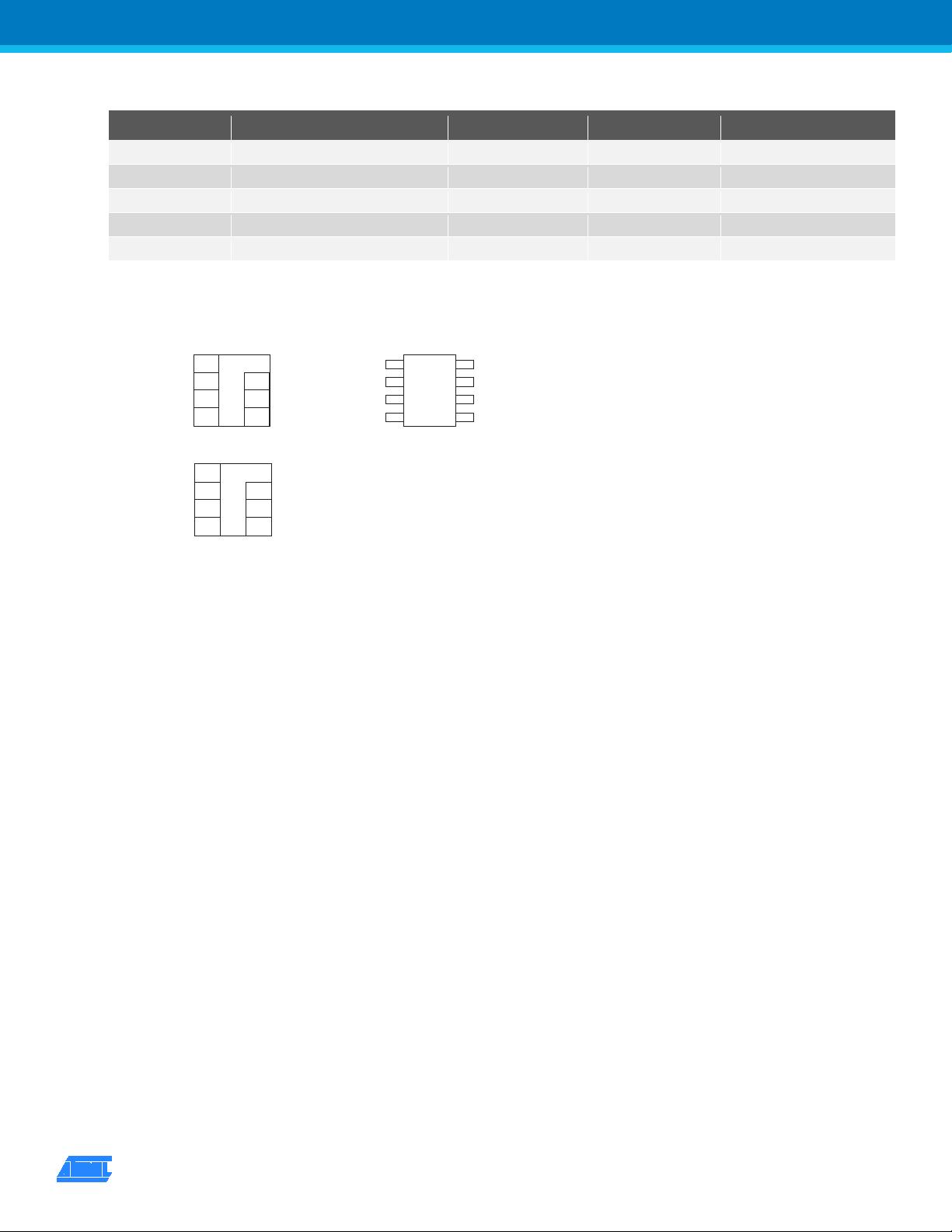
• Standard 8-lead plastic packages, green compliant (exceeds RoHS)
• Same pinout as two-wire Serial EEPROM's
• High reliability
• Endurance: 100,000 cycles
• Data retention: 10 years
• ESD protection: 4,000V min
* Note: Modules available with either T=0 / two-wire modes or two-wire mode only
2021LS−CRYPTO−11/11
This is a summary document.
The complete document is
available on the Atmel website
at www.atmel.com.
Atmel AT88SC0104C [SUMMARY DATASHEET]
2021LS−CRYPTO−11/11
2
Table 1. Pin Assignment
Pad
Description
ISO Module
TWI Module
Standard Package Pin
VCC Supply Voltage C1 C1 8
GND Ground C5 C5 4
SCL/CLK Serial Clock Input C3 C3 6
SDA/IO Serial Data Input/Output C7 C7 5
RST Reset Input C2 NC NC
Figure 1. Pin Configuration
V
CC
=C1
RST=C2
SCL/CLK=C3
NC=C4
ISO Smart Card Module
C5=GND
C6=NC
C7=SDA/IO
C8=NC
NC
NC
NC
GND
1
2
3
4
8
7
6
5
8-lead SOIC, PDIP
V
CC
NC
SCL
SDA
V
CC
=C1
NC=C2
SCL/CLK=C3
NC=C4
TWI Smart Card Module
C5=GND
C6=NC
C7=SDA/IO
C8=NC
1. Description
The Atmel
®
AT88SC0104C member of the Atmel CryptoMemory
®
family is a high-performance secure memory providing 1Kbit
of user memory with advanced security and cryptographic features built in. The user memory is divided into four 32-byte
zones, each of which may be individually set with different security access rights or effectively combined together to provide
space for one to four data files.
1.1 Smart Card Applications
The AT88SC0104C provides high security, low cost, and ease of implementation without the need for a microprocessor
operating system. The embedded cryptographic engine provides for dynamic and symmetric mutual authentication between
the device and host, as well as performing stream encryption for all data and passwords exchanged between the device and
host. Up to four unique key sets may be used for these operations. The AT88SC0104C offers the ability to communicate with
virtually any smart card reader using the asynchronous T = 0 protocol (Gemplus Patent) defined in ISO 7816-3.
1.2 Embedded Applications
Through dynamic and symmetric mutual authentication, data encryption, and the use of encrypted checksums, the
AT88SC0104C provides a secure place for storage of sensitive information within a system. With its tamper detection circuits,
this information remains safe even under attack. A two-wire serial interface running at 1.0MHz is used for fast and efficient
communications with up to 15 devices that may be individually addressed. The AT88SC0104C is available in industry standard
8-lead packages with the same familiar pinout as two-wire Serial EEPROMs.
Atmel AT88SC0104C [SUMMARY DATASHEET]
2021LS−CRYPTO−11/11
3
Figure 1-1. Block Diagram
Random
Generator
Authentication,
Encryption and
Certification Unit
EEPROM
Answer to Reset
Data Transfer
Password
Verification
Reset Block
Asynchronous
ISO Interface
Synchronous
Interface
Power
Management
V
CC
GND
SCL/CLK
SDA/IO
RST
2. Pin Descriptions
2.1 Supply Voltage (V
CC
)
The V
CC
input is a 2.7V to 5.5V positive voltage supplied by the host.
2.2 Clock (SCL/CLK)
In the asynchronous T = 0 protocol, the SCL/CLK input is used to provide the device with a carrier frequency f. The nominal
length of one bit emitted on I/O is defined as an “elementary time unit” (ETU) and is equal to 372/ f. When the synchronous
protocol is used, the SCL/CLK input is used to positive edge clock data into the device and negative edge clock data out of the
device.
2.3 Reset (RST)
The AT88SC0104C provides an ISO 7816-3 compliant asynchronous answer to reset sequence. When the reset sequence is
activated, the device will output the data programmed into the 64-bit answer-to-reset register. An internal pull-up on the RST
input pad allows the device to be used in synchronous mode without bonding RST. The AT88SC0104C does not support the
synchronous answer-to-reset sequence.
2.4 Serial Data (SDA/IO)
The SDA pin is bidirectional for serial data transfer. This pin is open-drain driven and may be wired with any number of other
open drain or open collector devices. An external pull-up resistor should be connected between SDA and V
CC
. The value of
this resistor and the system capacitance loading the SDA bus will determine the rise time of SDA. This rise time will determine
the maximum frequency during read operations. Low value pull-up resistors will allow higher frequency operations while
drawing higher average power. SDA/IO information applies to both asynchronous and synchronous protocols.
When the synchronous protocol is used, the SCL/CLK input is used to positive edge clock data into the device and negative
edge clock data out of the device.
Atmel AT88SC0104C [SUMMARY DATASHEET]
2021LS−CRYPTO−11/11
4
3. *Absolute Maximum Ratings
Operating Temperature .................. −40°C to +85°C
Storage Temperature .................. −65°C to + 150°C
Voltage on Any Pin
with Respect to Ground ............. − 0.7 to V
CC
+0.7V
Maximum Operating Voltage ........................... 6.0V
DC Output Current ........................................ 5.0mA
*
NOTICE: Stresses beyond those listed under “Absolute
Maximum Ratings” may cause permanent damage to
the device. This is a stress rating only and functional
operation of the device at these or any other condition
beyond those indicated in the operational sections of
this specification is not implied. Exposure to absolute
maximum rating conditions for extended periods of
time may affect device reliability.
Table 3-1. DC Characteristics
Applicable over recommended operating range from V
CC
= +2.7 to 5.5V, T
AC
= -40°C to +85°C (unless otherwise noted)
Symbol Parameter Test Condition Min Typ Max Units
V
CC
(2)
Supply Voltage 2.7 5.5 V
I
CC
Supply Current (V
CC
= 5.5V) Async Read at 3.57MHz 5 mA
I
CC
Supply Current (V
CC
= 5.5V) Async Write at 3.57MHz 5 mA
I
CC
Supply Current (V
CC
= 5.5V) Synch Read at 1MHz 5 mA
I
CC
Supply Current (V
CC
= 5.5V) Synch Write at 1MHz 5 mA
I
SB
Standby Current (V
CC
= 5.5V) V
IN
= V
CC
or GND 100 mA
V
IL
(1)
SDA/IO Input Low Threshold 0 V
CC
x 0.2 V
V
IL
(1)
SCL/CLK Input Low Threshold 0 V
CC
x 0.2 V
V
IL
(1)
RST Input Low Threshold 0 V
CC
x 0.2 V
V
IH
(1)(2)
SDA/IO Input High Threshold V
CC
x 0.7 V
CC
V
V
IH
(1)(2)
SCL/CLK Input High
Threshold
V
CC
x 0.7 V
CC
V
V
IH
(1)(2)
RST Input High Threshold V
CC
x 0.7 V
CC
V
I
IL
SDA/IO Input Low Current 0 < V
IL
< V
CC
x 0.15 15
µA
I
IL
SCL/CLK Input Low Current 0 < V
IL
< V
CC
x 0.15 15
µA
I
IL
RST Input Low Current 0 < V
IL
< V
CC
x 0.15 50
µA
I
IH
SDA/IO Input High Current V
CC
x 0.7 < V
IH
< V
CC
20
µA
I
IH
SCL/CLK Input High Current V
CC
x 0.7 < V
IH
< V
CC
100
µA
I
IH
RST Input High Current V
CC
x 0.7 < V
IH
< V
CC
150
µA
V
OH
SDA/IO Output High Voltage 20K ohm external pull-up V
CC
x 0.7 V
CC
V
V
OL
SDA/IO Output Low Voltage I
OL
= 1mA 0 V
CC
x 0.15 V
I
OH
SDA/IO Output High Current V
OH
20
µA
Notes: 1. V
IL
min and V
IH
max are reference only and are not tested
2. To prevent latch up conditions from occurring during power up of the AT88SCxxxxC, V
CC
must be turned on
before applying V
IH
. For powering down, V
IH
must be removed before turning V
CC
off
剩余19页未读,继续阅读
资源评论
- dcsn6112015-08-31刚好需要。不过在atmel官网上也可以下载
BarberOfSiberia
- 粉丝: 0
- 资源: 2
上传资源 快速赚钱
- 我的内容管理 展开
- 我的资源 快来上传第一个资源
- 我的收益 登录查看自己的收益
- 我的积分 登录查看自己的积分
- 我的C币 登录后查看C币余额
- 我的收藏
- 我的下载
- 下载帮助
安全验证
文档复制为VIP权益,开通VIP直接复制
信息提交成功