没有合适的资源?快使用搜索试试~ 我知道了~
资源推荐
资源详情
资源评论
RDA8851CL Datasheet V1.05
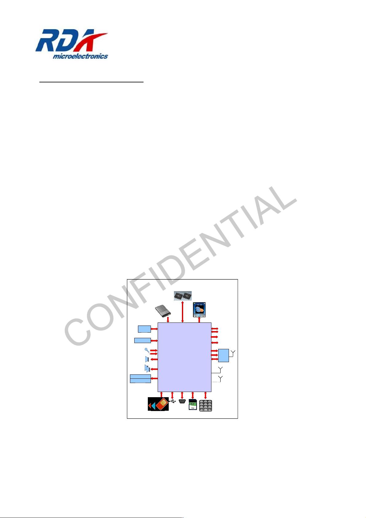
RDA8851CL GSM/GPRS Single-Chip Terminal
RDA Microelectronics Inc. CONFIDENTIAL 1 / 100
● Connectivity
USB 1.1 Device
2 UART interface
1 SD controller
1 SD/SPI controller
SPI with multiple chip select
I2C controller
General Purpose I/Os
2 GPADC, 10bits, 2 channels
● Audio
2 channels voice ADC, 8kHz, 13 bits/sample
for headset and on-board microphone
Voice DAC, 8kHz, 13 bits/sample for
receiver
High fidelity Stereo DAC, up to 48kHz, 16
bits per sample
Stereo Audio speaker driver
1.5W differential output stereo amplifier for
loudspeaker, Class K
Stereo analog audio line input
● Debug
Host debug interface allowing non intrusive
in depth investigation
GDB debugger
Execution logger and profiling through debug
port
High level text based debugging using Host
debug or USB
● FM
Integrated Broadcast FM tuner which can be
tuned world-wide frequency band
● Bluetooth
Integrated Bluetooth SoC complaint with 2.1
+ EDR standard
APPLICATIONS
Multi-band GSM/GPRS Mobile Handsets, PDAs,
data terminals and Modems: GSM 850, GSM
900, DCS1800, PCS 1900.
The high level of integration achieved on
RDA8851CL allows for highly featured phone without
increasing the BOM.
FEATURES
● External Memory Interface
Integrated 32Mb 1.8V Flash on chip, and also
Supports external SPI Flash
Integrated PSRAM on chip, 64Mb size
Power efficient using retention technology to
avoid floating lines
Flexible IO voltage
● GSM/GPRS Modem
GPRS Class 10
Quad bands integrated transceiver
Supports HR, FR, EFR, AMR voice codec
Triple SIM controller with integrated level shifters
Provide a complete GSM/GPRS data path with
integrated RF transceiver, Saw-Less, only needs
external PA
● Multimedia
Support camera interface up to 3Mpix sensors
with 8 bit parallel or 1/2/4 data series
interface,Support CSI camera interface
Support LCD module interface with 8 bit parallel
interface or SPI series interface
Support up to 480X640 resolution
4-layers blending graphical engine capable of
resizing and YUV2RGB conversion
Proprietary 16/32-bit digital signal processing
engine to improve computation performance
● Power Management
Power On reset control
Internal 32K OSC for standby/ shutoff/ sleep state
Battery charger (from USB or AC charger)
Integrated all internal voltages from VBAT
Provide all LDOs for external components
● User Interface
8x8 Keypad scanner with multiple key detection,
support ADC serial interface Keypad
Alerter
Light Pulse Generator for blinking LED
Pulse Width Modulator for Keyboard or backlight
control
Touch screen interface
LED drivers for LCD and keyboard backlight
Calendar (Real Time Clock) with alarm
RDA8851CL Datasheet V1.05
GENERAL DESCRIPTION
A high performance, high integrated system-on-chip solution for low cost, low power GSM/GPRS mobile phones.
RDA8851CL is a high performance, highly integrated system-on-chip solution for low cost, low power,
GSM/GPRS mobile phone.
Integrating all essential electronic components, including baseband, quad band RF transceiver, power
management, FM receiver onto a single system on chip, RDA8851CL offers best in class bill of material, space
requirement and cost/feature ratio for complete phone handsets.
Built around a cost effective 32-bit XCPU RISC core running at up to 312MHz with 4k of Instruction cache and
4k of Data cache, RDA8851CL offers plenty of processing power for multimedia applications. A high
performance proprietary 16/32-bit digital signal processing engine can further improve overall performance and
user experience when performing complex multimedia tasks.
It is also packed with impressive connectivity for easy scalability of the system, allowing glue less interfaces to
camera and multimedia companion chips, SDMMC Memory Cards and SPI devices, LCD modules and USB
(slave, full speed).
RDA8851CL is GPRS Class 10 enabled, and supports Full Rate (FR), Half Rate (HR), Enhanced Full Rate
(EFR) and Adaptive Multi Rate (AMR) voice coders. It also supports simultaneous dual network operation and
integrates a SIM controller with integrated level shifters that can support three SIM cards.
Additionally, RDA8851CL integrates a FM tuner and a Bluetooth module which completely include digital,
analogue and RF function. And they can easily work only with a few passive components as filter or matching
network..
RDA8851CL is available in a small footprint, fine pitch, 12 X10, 203 ball TFBGA package.
RDA Microelectronics Inc. CONFIDENTIAL 2 / 100
Figure 1: RDA8851CL Typical
Application
Typical Application
Triple
SIM
GSM RF Port
HST
Parallel/Series
PWL/PWT
LED Drivers
Bluetooth
RF Port
Headset Stereo Out
Loudspeaker Out
Receiver Out
Headset MIC
Onboard MIC
Coolhost
debugger
LCD Back light
GPIO
32k OSC
32K/26M CLK_OUT
LCD
Camera Sensor
26M OSC
PA /
Switch
GSM PA Level
TCO
FM RF Port
SD
MMC
UART
IrDA
USB 1.1
Key Back light
SPI
VBAT
KEYPAD
Matrix
RDA8851CL Datasheet V1.05
Table of Contents
Features ................................................................................................................................................................1
Applications ...........................................................................................................................................................1
General Description ..............................................................................................................................................2
A. Architecture Overview ......................................................................................................................................6
B. Block Description ...........................................................................................................................................14
B.I System Modules ......................................................................................................................................14
B.I.1 System CPU (XCPU) .......................................................................................................................14
B.I.2 Memory Bridge ................................................................................................................................22
Operations ...........................................................................................................................................23
B.I.3 Direct Memory Access (DMA) ..........................................................................................................24
B.I.4 Page Spy .........................................................................................................................................25
B.I.5 System Intelligent Flow Controller (Sys IFC) ....................................................................................25
AHB2APB bridge operation ..................................................................................................................26
DMA Operations ..................................................................................................................................26
RF_SPI channel ...................................................................................................................................27
Debug channel operations ...................................................................................................................27
B.II System Peripherals .................................................................................................................................28
B.II.1 System and Clock Control ..............................................................................................................28
B.II.2 Trace (Normal UART) and Host (Debug UART) Port .....................................................................30
B.II.3 Serial Peripheral Interface (SPI) .....................................................................................................36
B.II.4 I2C ..................................................................................................................................................36
B.II.5 Serial Peripheral Interface for RF (RF SPI) .....................................................................................38
B.II.6 General Purpose Input Output .......................................................................................................39
B.II.7 Keypad ...........................................................................................................................................39
B.II.8 Pulse Width Modulation (PWM) ......................................................................................................40
B.II.9 Sim Card Interface (SCI) ................................................................................................................40
B.II.10 Calendar .......................................................................................................................................41
B.II.11 Timers ..........................................................................................................................................41
B.II.12 Debug Port (EXL, PXTS, Signal Spy) ...........................................................................................42
B.II.13 General Purpose Analog to Digital Converter (GP ADC) ..............................................................42
B.II.14 Timing Control Unit and Low Power Synchronizer (TCU+LPS) .....................................................43
B.II.15 System AHB Monitor (Sys AHBC Mon) and Base Band AHB Monitor (BB AHBC Mon) ...............44
B.II.16 System IRQ Controller (Sys IRQ) .................................................................................................44
B.II.17 USB Controller ..............................................................................................................................45
B.II.18 Graphic Overlay United Display Accelerator (GOUDA) .................................................................45
B.II.19 Camera Controller ........................................................................................................................46
B.II.20 SD/MMC Controller .......................................................................................................................49
B.II.21 Audio Interface Analog + I2S (AIF) ...............................................................................................49
B.III Base Band Modules ...............................................................................................................................50
B.III.1 GSM / GPRS Modem ....................................................................................................................50
RDA Microelectronics Inc. CONFIDENTIAL 3 / 100
RDA8851CL Datasheet V1.05
B.III.2 Voice Coprocessor (VoC) ..............................................................................................................50
B.IV Baseband Peripherals ...........................................................................................................................51
B.IV.1 DIGRF Interface (RF IF) ................................................................................................................51
B.V Analog Modules ......................................................................................................................................51
SPI Interface for Analog IP control .......................................................................................................52
Power Management Unit ......................................................................................................................52
Analog BaseBand (ABB) ......................................................................................................................58
RF Transceiver ....................................................................................................................................62
J.I FM ............................................................................................................................................................63
General Description .............................................................................................................................64
Features ...............................................................................................................................................64
Block Description .................................................................................................................................64
Receiver Characteristics ......................................................................................................................65
J.II Bluetooth .................................................................................................................................................66
General Description .............................................................................................................................66
Features ...............................................................................................................................................67
Block Description .................................................................................................................................67
Performance Characteristics ................................................................................................................68
K. Memory Map ..................................................................................................................................................71
L. Pins Description .............................................................................................................................................74
L.I Pin-out ......................................................................................................................................................74
M. Electrical Characteristics ...............................................................................................................................81
M.I Absolute Maximum Rating ......................................................................................................................81
M.II Temperature Characteristics ..................................................................................................................81
M.III RF Characteristics .................................................................................................................................81
M.IV Audio Characteristics ............................................................................................................................83
M.VI DC Characteristics ................................................................................................................................84
M.VII Digital IO DC Characteristics ...............................................................................................................94
M.VIII Digital IO AC Characteristics (SPI Interface Timing) ...........................................................................94
N. Packaging ......................................................................................................................................................97
O. Ball Out .........................................................................................................................................................98
P. Glossary ........................................................................................................................................................99
RDA Microelectronics Inc. CONFIDENTIAL 4 / 100
RDA8851CL Datasheet V1.05
Figure Index
Figure 1: RDA8851CL Typical Application ...................................................................................................2
Figure A.1 RDA8851CL Integrated IPs & Interfaces ..................................................................................6
Figure A.2: Digital Baseband Diagram .........................................................................................................9
Figure B.1: XCPU Block Diagram ..............................................................................................................15
Figure B.2: Typical transfer operation ........................................................................................................26
Figure B.3: Debug channel block diagram .................................................................................................28
Figure B.4: General Message Format ........................................................................................................32
Figure B.5: Read Return Message Format ................................................................................................32
Figure B.6: Event Message Format ...........................................................................................................32
Figure B.7: Tx Switch STM ........................................................................................................................34
Figure B.8: IrDA SIR Data Format .............................................................................................................34
Figure B.9: YUV 4:2:2 Subsampling ...........................................................................................................47
Figure B.10: SPI Write & Read Timing .......................................................................................................52
Figure B.11: PMU Power ON .....................................................................................................................53
Figure B.12: POR triggered by POWKEY press ........................................................................................54
Figure B.13: Principle schematic for Power-Profiles usage ........................................................................55
Figure B.14: Charging I-V Curve ................................................................................................................57
Figure B.15: PLL Clock Path ......................................................................................................................59
Figure B.16: Audio Analog IP .....................................................................................................................60
Figure B.17: USB PHY FS 1.1 ..................................................................................................................61
Figure B.18: GPADC Timing Diagram .......................................................................................................62
Figure B.19: RF transceiver block digram ..................................................................................................63
Figure B.20: FM Tuner Block Diagram .......................................................................................................65
Figure B.21: Bluetooth Block Diagram .......................................................................................................67
Figure M.1: SCLK Timing Diagram ............................................................................................................95
Figure M.2: SPI Write Timing Diagram .....................................................................................................96
Figure M.3: SPI Read Timing Diagram ......................................................................................................96
Figure O.1: RDA8851CL Ball out diagram ................................................................................................98
RDA Microelectronics Inc. CONFIDENTIAL 5 / 100
剩余99页未读,继续阅读
资源评论
styliter
- 粉丝: 0
- 资源: 1
上传资源 快速赚钱
- 我的内容管理 展开
- 我的资源 快来上传第一个资源
- 我的收益 登录查看自己的收益
- 我的积分 登录查看自己的积分
- 我的C币 登录后查看C币余额
- 我的收藏
- 我的下载
- 下载帮助
安全验证
文档复制为VIP权益,开通VIP直接复制
信息提交成功