


1 Chapter 6 Problem Set
Chapter 6
PROBLEMS
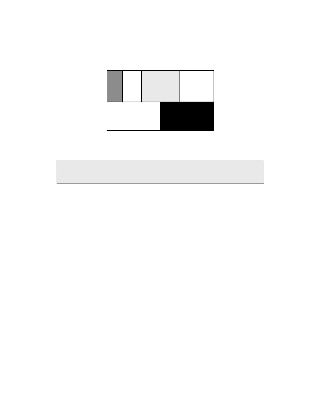
1. [E, None, 4.2] Implement the equation X = ((A + B) (C + D + E) + F) G using complemen-
tary CMOS. Size the devices so that the output resistance is the same as that of an inverter
with an NMOS W/L = 2 and PMOS W/L = 6. Which input pattern(s) would give the worst and
best equivalent pull-up or pull-down resistance?
Solution
Rewriting the output expression in the form X = ((A + B) (C + D + E) + F) G = ((AB +
CDE)F) + G allows us to build the pulldown network by inspection (parallel devices imple-
ment an OR, and series devices implement an AND). The pullup network is the dual of the
pulldown network.
The plot shows sizes that meet the requirement - in the worst case, the output resistance
of the circuit matches the output resistance of an inverter with NMOS W/L=2 and PMOS
W/L=6.
The worst case pull-up resistance occurs whenever a single path exists from the output
node to Vdd. Examples of vectors for the worst case are ABCDEFG=1111100 and 0101110.
The best case pull-up resistance occurs when ABCDEFG=0000000.
The worst case pull-down resistance occurs whenever a single path exists from the out-
put node to GND. Examples of vectors for the worst case are ABCDEFG=0000001 and
0011110.
The best case pull-down resistance occurs when ABCDEFG=1111111.
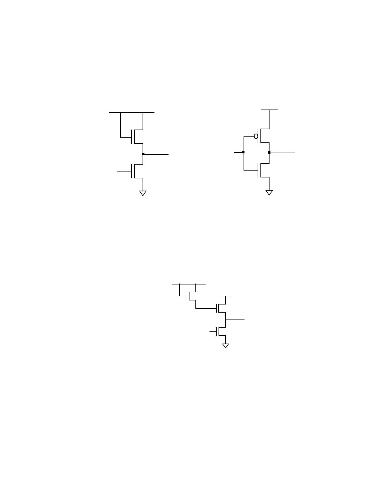
2. Implement the following expression in a full static CMOS logic fashion using no more than
10 transistors:
Solution
A
B
F
C
D
E
G
F
G
C
D E
A
B
X
2
4
12
12
12
8
8
12
12
2424
24 2424
YAB⋅()ACE⋅⋅()DE⋅()DCB⋅⋅()+++=


- 1
- 2
- 3
- 4
- 5
- 6
前往页