没有合适的资源?快使用搜索试试~ 我知道了~
AWR1243 Cascade.pdf
需积分: 5 15 下载量 89 浏览量
2020-05-31
21:52:14
上传
评论 1
收藏 242KB PDF 举报
温馨提示
试读
15页
TI的12发16收MIMO雷达方案,毫米波MIMO雷达会是将来汽车雷达的一种方向,该方案是德州仪器给市场的解决方案
资源推荐
资源详情
资源评论
1
SWRA574A–October 2017–Revised December 2017
Submit Documentation Feedback
Copyright © 2017, Texas Instruments Incorporated
AWR1243 Cascade
Application Report
SWRA574A–October 2017–Revised December 2017
AWR1243 Cascade
Anil Kumar K V, Sreekiran, Samala, Karthik Subburaj, Chethan Kumar Y.B.
ABSTRACT
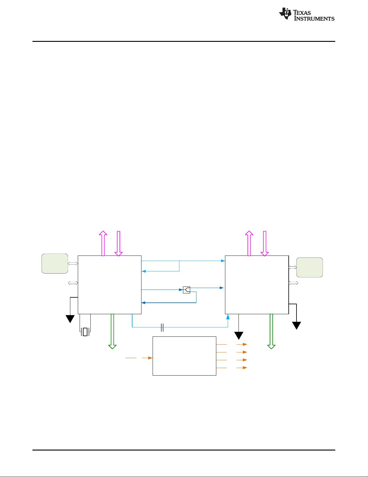
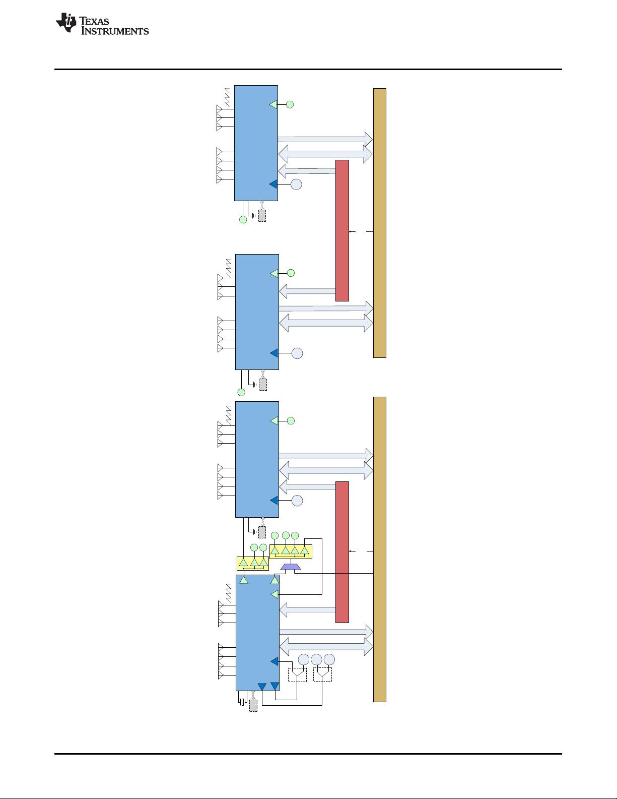
This application report describes TI’s cascaded mmWave radar system. This solution is based on TI’s
AWR1243 radar chip. Several of these chips are cascaded and operated in synchronism. Each AWR1243
chip supports up to four receive and three transmit antennas. Cascading multiple such chips allows the
radar system to operate with more receive and transmit antennas, thereby improving target detection and
resolution in comparison with a single AWR1243 radar chip based system. Cascading of two and four
AWR1243 chips is illustrated in this application note, targeting automotive applications such as Adaptive
Cruise Control, Collision Warning, Emergency Braking, and Semi and Fully Autonomous Driving.
Contents
1 Cascaded AWR1243 System ............................................................................................. 2
2 Synchronization of AWR1243 Chips ...................................................................................... 4
3 Connectivity................................................................................................................... 8
4 20 GHz LO Sync Link Budget.............................................................................................. 9
5 Software Messaging ....................................................................................................... 10
6 Advantages of AWR1243 Cascading System ......................................................................... 13
7 References .................................................................................................................. 13
List of Figures
1 A Two Chip Cascade System.............................................................................................. 2
2 A Four Chip Cascade System ............................................................................................. 3
3 20 GHz Mux Options in the Chip .......................................................................................... 4
4 Example of LO Distribution in 2-Chip Star Topology.................................................................... 5
5 Frame (Burst) Timing and Clock Generation in AWR1243............................................................. 6
6 Frame (Burst) Timing Generation in Two Chip Cascade Example ................................................... 7
7 20 GHz LO - Link Budget................................................................................................... 9
List of Tables
1 DIG_SYNC_IN Imbalance Summary...................................................................................... 8
2 Recommended Combinations of Pins to be Used in 20 GHz LO ..................................................... 8
3 Channel Configuration Message ......................................................................................... 11
4 Profile Configuration Message ........................................................................................... 11
5 Chirp Configuration Message............................................................................................. 12
6 Frame Configuration Message ........................................................................................... 12
AWR1243
PM circuits
1.0V
1.8V
1.2V
3.3V
Master
Slave
CLKP
5V
CSI2 DATA, CLK
OR
LVDS DATA, CLK
SFlash
SFlash
OSC_CLKOUT
CLKM
SYNC_OUT
SYNC_IN
AWR1243
FM_CW_SYNCOUT
FM_CW_SYNCIN1/
FM_CW_SYNCIN2
20GHz
40MHz
40MHz
FM_CW_SYNCIN1
CLKM
CLKP
To Antenna
RX1, 2, 3, 4
TX1, 2, 3
To Antenna
RX1, 2, 3, 4
TX1, 2, 3
SPI interface
SPI interface
SYNC_IN
(For development
only)
(For development
only)
CSI2 DATA, CLK
OR
LVDS DATA, CLK
FM_CW_SYNCIN2
FM_CW_SYNCIN2/
FM_CW_SYNCIN1
Cascaded AWR1243 System
www.ti.com
2
SWRA574A–October 2017–Revised December 2017
Submit Documentation Feedback
Copyright © 2017, Texas Instruments Incorporated
AWR1243 Cascade
Trademarks
All trademarks are the property of their respective owners.
1 Cascaded AWR1243 System
Multiple AWR1243 chips may be cascaded on PCB to improve target detection and resolution. In this
section, two chip cascading and four chip cascading are illustrated as examples. The focus is on
connection of various signals that the AWR1243 chips need to share among themselves. Of the multiple
AWR1243 chips in the cascaded system, one is referred to as the Master and the others as Slaves. To
make the entire cascaded system operate as a single radar system, the Master is designated to generate
a common ~20 GHz Local Oscillator (LO) signal shared across all the transmitters and receivers in the
entire cascade system. The master also controls the radar chirp/frame timing for all the chips by
generating a digital Sync signal and sharing then with the slaves. The master also uses a 40 MHz crystal
and generates a 40 MHz oscillator clock (OSC_CLKOUT) and shares it with the slaves (as CLKP),
thereby obviating the need for additional crystals on the slaves and ensuring that the entire system
operates on a single root clock.
The master is capable of supplying the ~20 GHz LO on two different output pins through two different
delay matched amplifiers. This can be used in a four chip cascade system to supply the LO signal to the
master and three slaves using just passive splitters and without additional active components on board.
The OSC_CLKOUT is conveyed from the master to the slaves through buffers on board. The DIG_SYNC
is conveyed from the master to the slaves and back to itself through delay matched buffers on board.
Other than these connections which are illustrated in the below diagrams and further elaborated in later
sections, the cascaded system also has Power Management ICs (PMIC) (each PMIC can cater to two
AWR1243 chips), an optional QSPI Flash (needed for initial software development purpose only) and the
mmWave antennas connected to each AWR1243 chip.
Figure 1. A Two Chip Cascade System
4 Supply Rails
High Speed CSI
2
Signals
High speed CSI
2
Signals
High Speed CSI2 Signals
4 Supply Rails
AWR1243 Master
Power Management
IC
(LP87524)
Clock Driver
Sync Driver
Control Signal and Data Capture Signals
Control Signals
AWR1243 Slave
QSPI
Flash
Control Signals
A
A
C
B
D
E
CLKP
CLKP
CLKM
GND
F
F
G
H
OSC_CLKOUT
Sync_out
CLKM
Sync_in
Sync_in
RX Antennas TX Antennas
AWR1243 Slave
QSPI
Flash
4 Supply Rails
Control Signals
B
CLKP
CLKM
GND
G
Sync_in
RX Antennas TX Antennas
Control Signal and Data Capture Signals
AWR1243 Slave
QSPI
Flash
4
Supply Rails
Control Signals
C
CLKP
CLKM
GND
H
Sync_in
RX Antennas TX Antennas
D
E
FMCW
CLKOUT
FMCW
SYNCOUT
FMCW
SYNCIN
FMCW
SYNCIN
FMCW
SYNCIN
FMCW
SYNCIN
Power Splitter
For Development Only
QSPI
Flash
5V Input
5V Input
M
U
X
3.3V,1.2V, 1.8V & 1.0V 3.3V, 1.2V, 1.8V & 1.0V
Power Management
IC
(LP87524)
3.3V,1.2V, 1.8V & 1.0V 3.3V, 1.2V, 1.8V & 1.0V
For Development Only
External Sync_in
Copyright © 2017, Texas Instruments Incorporated
www.ti.com
Cascaded AWR1243 System
3
SWRA574A–October 2017–Revised December 2017
Submit Documentation Feedback
Copyright © 2017, Texas Instruments Incorporated
AWR1243 Cascade
Figure 2. A Four Chip Cascade System
剩余14页未读,继续阅读
资源评论
星海灵南
- 粉丝: 0
- 资源: 10
上传资源 快速赚钱
- 我的内容管理 展开
- 我的资源 快来上传第一个资源
- 我的收益 登录查看自己的收益
- 我的积分 登录查看自己的积分
- 我的C币 登录后查看C币余额
- 我的收藏
- 我的下载
- 下载帮助
安全验证
文档复制为VIP权益,开通VIP直接复制
信息提交成功