
IMX274LQC-C
5
Contents
Description -------------------------------------------------------------------------------------------------------------------------------------------- 1
Features ----------------------------------------------------------------------------------------------------------------------------------------------- 1
Device Structure ------------------------------------------------------------------------------------------------------------------------------------- 2
Optical Black Array and Readout Scan Direction --------------------------------------------------------------------------------------------- 2
Absolute Maximum Ratings ----------------------------------------------------------------------------------------------------------------------- 3
Recommended Operating Conditions ----------------------------------------------------------------------------------------------------------- 3
USE RESTRICTION NOTICE -------------------------------------------------------------------------------------------------------------------- 4
Contents ----------------------------------------------------------------------------------------------------------------------------------------------- 5
Optical Center ---------------------------------------------------------------------------------------------------------------------------------------- 8
Pin Configuration ------------------------------------------------------------------------------------------------------------------------------------ 8
Pin Description --------------------------------------------------------------------------------------------------------------------------------------- 9
When using CSI-2 ........................................................................................................................................................9
When using Sub-LVDS ............................................................................................................................................... 12
I/O Equivalent Circuit Diagram-------------------------------------------------------------------------------------------------------------------15
Peripheral Circuit -----------------------------------------------------------------------------------------------------------------------------------19
System Outline --------------------------------------------------------------------------------------------------------------------------------------20
When using CSI-2 ...................................................................................................................................................... 20
When using Sub-LVDS ............................................................................................................................................... 20
Electrical Characteristics when using CSI-2 --------------------------------------------------------------------------------------------------21
1. DC Characteristics (CSI-2) ...................................................................................................................................... 21
Current Consumption and Gain Variable Range (CSI-2) ........................................................................................... 21
Supply Voltage and I/O Voltage (CSI-2) ................................................................................................................... 21
2. AC Characteristics (CSI-2) ...................................................................................................................................... 22
INCK, XCLR (CSI-2) ............................................................................................................................................... 22
XHS, XVS (Output) (CSI-2) ..................................................................................................................................... 22
I
2
C Communication (CSI-2) ..................................................................................................................................... 23
DMCKP / DMCKN,DMO (CSI-2)............................................................................................................................ 23
Electrical Characteristics When Using Sub-LVDS -------------------------------------------------------------------------------------------24
1. DC Characteristics (Sub-LVDS) .............................................................................................................................. 24
Current Consumption and Gain Variable Range (Sub-LVDS) .................................................................................... 24
Supply Voltage and I/O Voltage (Sub-LVDS) ............................................................................................................ 24
LVDS Output DC Characteristics (Sub-LVDS) .......................................................................................................... 24
2. AC Characteristics (Sub-LVDS) ............................................................................................................................... 25
INCK, XCLR, XVS (input), XHS (input) (Sub-LVDS) ................................................................................................. 25
Serial Communication (Sub-LVDS) .......................................................................................................................... 25
Sub-LVDS Output (Sub-LVDS) ................................................................................................................................ 26
Spectral Sensitivity Characteristics (CSI-2 and Sub-LVDS) -------------------------------------------------------------------------------27
Image Sensor Characteristics (CSI-2 and Sub-LVDS)--------------------------------------------------------------------------------------28
1. Zone Definition of Image Sensor Characteristics...................................................................................................... 28
Image Sensor Characteristics Measurement Method (CSI-2 and Sub-LVDS) ---------------------------------------------------------29
1. Measurement Conditions ........................................................................................................................................ 29
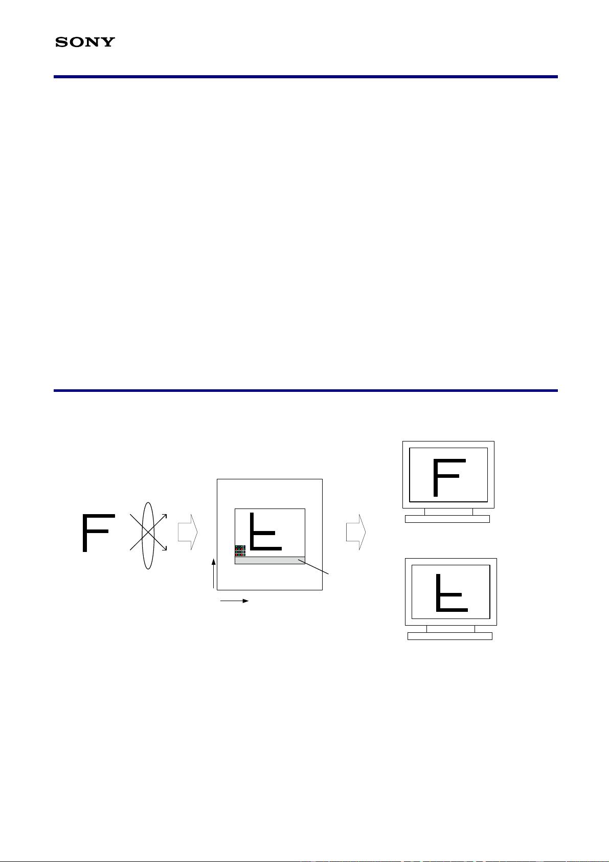
2. Color Coding of this Image Sensor and Readout ..................................................................................................... 29
3. Definition of Standard Imaging Conditions ............................................................................................................... 29
Setting Registers Using I
2
C Communication (When Using CSI-2) -----------------------------------------------------------------------31
Description of Setting Registers When Using I
2
C Communication ................................................................................ 31
Pin Connection of Serial Communication Operation Specifications When Using I
2
C Communication ............................. 31
Register Communication Timing When Using I
2
C Communication ................................................................................ 31
I
2
C Communication Protocol ....................................................................................................................................... 32
Register Write and Read ............................................................................................................................................ 33
Single Read from Random Location ........................................................................................................................ 33
Single Read from Current Location .......................................................................................................................... 33
Sequential Read Starting from Random Location ..................................................................................................... 34
Sequential Read Starting from Current Location ....................................................................................................... 34
Single Write to Random Location ............................................................................................................................. 35
Sequential Write Starting from Random Location ..................................................................................................... 35
Register Value Reflection Timing to Output Data (CSI-2) ............................................................................................. 36


- 1
- 2
前往页