没有合适的资源?快使用搜索试试~ 我知道了~
资源推荐
资源详情
资源评论


________________General Description
The MAX192 is a low-cost, 10-bit data-acquisition system
that combines an 8-channel multiplexer, high-bandwidth
track/hold, and serial interface with high conversion
speed and ultra-low power consumption. The device
operates with a single +5V supply. The analog inputs are
software configurable for single-ended and differential
(unipolar/bipolar) operation.
The 4-wire serial interface connects directly to SPI™,
QSPI™, and Microwire™ devices, without using external
logic. A serial strobe output allows direct connection to
TMS320 family digital signal processors. The MAX192
uses either the internal clock or an external serial-
interface clock to perform successive approximation A/D
conversions. The serial interface can operate beyond
4MHz when the internal clock is used. The MAX192 has
an internal 4.096V reference with a drift of ±30ppm typi-
cal. A reference-buffer amplifier simplifies gain trim and
two sub-LSBs reduce quantization errors.
The MAX192 provides a hardwired SHDN pin and two
software-selectable power-down modes. Accessing the
serial interface automatically powers up the device, and
the quick turn-on time allows the MAX192 to be shut
down between conversions. By powering down
between conversions, supply current can be cut to
under 10µA at reduced sampling rates.
The MAX192 is available in 20-pin DIP and SO pack-
ages, and in a shrink-small-outline package (SSOP)
that occupies 30% less area than an 8-pin DIP. The
data format provides hardware and software compati-
bility with the MAX186/MAX188. For anti-aliasing filters,
consult the data sheets for the MAX291–MAX297.
________________________Applications
Automotive
Pen-Entry Systems
Consumer Electronics
Portable Data Logging
Robotics
Battery-Powered Instruments, Battery
Management
Medical Instruments
____________________________Features
♦ 8-Channel Single-Ended or 4-Channel Differential
Inputs
♦ Single +5V Operation
♦ Low Power: 1.5mA (operating)
2µA (power-down)
♦ Internal Track/Hold, 133kHz Sampling Rate
♦ Internal 4.096V Reference
♦ 4-Wire Serial Interface is Compatible
with SPI, QSPI, Microwire, and TMS320
♦ 20-Pin DIP, SO, SSOP Packages
♦ Pin-Compatible 12-Bit Upgrade (MAX186/MAX188)
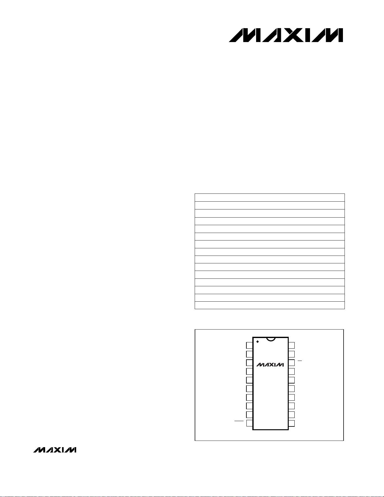
_______________Ordering Information
MAX192
Low-Power, 8-Channel,
Serial 10-Bit ADC
________________________________________________________________ Maxim Integrated Products
1
20
19
18
17
16
15
14
13
12
11
1
2
3
4
5
6
7
8
9
10
TOP VIEW
DIP/SO/SSOP
V
DD
SCLK
CS
DIN
SSTRB
DOUT
DGND
AGND
REFADJ
VREFSHDN
AGND
CH7
CH6
CH5
CH4
CH3
CH2
CH1
CH0
MAX192
___________________Pin Configuration
SPI and QSPI are trademarks of Motorola Corp.
Microwire is a trademark of National Semiconductor Corp.
19-0247; Rev. 1; 4/97
PART TEMP. RANGE
MAX192ACPP 0°C to +70°C
MAX192BCPP 0°C to +70°C
MAX192ACWP 0°C to +70°C 20 Wide SO
20 Plastic DIP
20 Plastic DIP
PIN-PACKAGE
MAX192BCWP 0°C to +70°C 20 Wide SO
MAX192ACAP 0°C to +70°C 20 SSOP
MAX192BCAP 0°C to +70°C 20 SSOP
±1/2
±1
±1/2
INL (LSB)
±1
±1/2
±1
MAX192AEPP -40°C to +85°C 20 Plastic DIP ±1/2
MAX192BEPP -40°C to +85°C 20 Plastic DIP ±1
MAX192AEWP -40°C to +85°C 20 Wide SO ±1/2
MAX192BEWP -40°C to +85°C 20 Wide SO ±1
MAX192AEAP -40°C to +85°C 20 SSOP ±1/2
MAX192BEAP -40°C to +85°C 20 SSOP ±1
MAX192AMJP -55°C to +125°C 20 CERDIP ±1/2
MAX192BMJP -55°C to +125°C 20 CERDIP ±1
See last page for Typical Operating Circuit.
For free samples & the latest literature: http://www.maxim-ic.com, or phone 1-800-998-8800.
For small orders, phone 408-737-7600 ext. 3468.

MAX192
Low-Power, 8-Channel,
Serial 10-Bit ADC
2 _______________________________________________________________________________________
V
DD
to AGND........................................................... -0.3V to +6V
AGND to DGND.................................................... -0.3V to +0.3V
CH0–CH7 to AGND, DGND ...................... -0.3V to (V
DD
+ 0.3V)
CH0–CH7 Total Input Current.......................................... ±20mA
VREF to AGND .......................................... -0.3V to (V
DD
+ 0.3V)
REFADJ to AGND...................................... -0.3V to (V
DD
+ 0.3V)
Digital Inputs to DGND.............................. -0.3V to (V
DD
+ 0.3V)
Digital Outputs to DGND........................... -0.3V to (V
DD
+ 0.3V)
Digital Output Sink Current .................................................25mA
Continuous Power Dissipation (T
A
= +70°C)
Plastic DIP (derate 11.11mW/°C above +70°C) ......... 889mW
SO (derate 10.00mW/°C above +70°C)...................... 800mW
SSOP (derate 8.00mW/°C above +70°C) ................... 640mW
CERDIP (derate 11.11mW/°C above +70°C).............. 889mW
Operating Temperature Ranges
MAX192_C_P ..................................................... 0°C to +70°C
MAX192_E_P .................................................. -40°C to +85°C
MAX192_MJP ............................................... -55°C to +125°C
Storage Temperature Range ............................ -60°C to +150°C
Lead Temperature (soldering, 10sec) ............................ +300°C
ELECTRICAL CHARACTERISTICS
(V
DD
= 5V ±5%, f
CLK
= 2.0MHz, external clock (50% duty cycle), 15 clocks/conversion cycle (133ksps), 4.7µF capacitor at VREF pin,
T
A
= T
MIN
to T
MAX,
unless otherwise noted. Typical values are at T
A
= +25°C.)
Stresses beyond those listed under “Absolute Maximum Ratings” may cause permanent damage to the device. These are stress ratings only, and functional
operation of the device at these or any other conditions beyond those indicated in the operational sections of the specifications is not implied. Exposure to
absolute maximum rating conditions for extended periods may affect device reliability.
ABSOLUTE MAXIMUM RATINGS
MAX192A
-3dB rolloff
65kHz, V
IN
= 4.096Vp-p (Note 3)
External reference, 4.096V
MAX192B
No missing codes over temperature
External reference, 4.096V
CONDITIONS
kHz800Full-Power Bandwidth
MHz4.5Small-Signal Bandwidth
dB-75Channel-to-Channel Crosstalk
dB70SFDRSpurious-Free Dynamic Range
dB-70THD
Total Harmonic Distortion
(up to the 5th harmonic)
dB66SINADSignal-to-Noise + Distortion Ratio
±1/2
Bits10Resolution
LSB±0.1
Channel-to-Channel
Offset Matching
ppm/°C±0.8Gain Temperature Coefficient
LSB
±1
Relative Accuracy (Note 2)
LSB±1DNLDifferential Nonlinearity
LSB±2Offset Error
LSB±2Gain Error
UNITSMIN TYP MAXSYMBOLPARAMETER
Internal clock 5.5 10
Conversion Time (Note 4) t
CONV
External clock, 2MHz, 12 clocks/conversion 6
µs
Track/Hold Acquisition Time t
AZ
1.5 µs
Aperture Delay 10 ns
Aperture Jitter <50 ps
Internal Clock Frequency 1.7 MHz
DC ACCURACY (Note 1)
DYNAMIC SPECIFICATIONS (10kHz sine-wave input, 4.096Vp-p, 133ksps, 2.0MHz external clock)
CONVERSION RATE

MAX192
Low-Power, 8-Channel,
Serial 10-Bit ADC
_______________________________________________________________________________________ 3
ELECTRICAL CHARACTERISTICS (continued)
(V
DD
= 5V ±5%, f
CLK
= 2.0MHz, external clock (50% duty cycle), 15 clocks/conversion cycle (133ksps), 4.7µF capacitor at VREF pin,
T
A
= T
MIN
to T
MAX,
unless otherwise noted. Typical values are at T
A
= +25°C.)
Internal compensation
0mA to 0.5mA output load
T
A
= +25°C (Note 7)
(Note 5)
On/off leakage current; V
IN
= 0V, 5V
Bipolar
Used for data transfer only
Internal compensation (Note 5)
External compensation, 4.7µF
Single-ended range (unipolar only)
Common-mode range (any input)
CONDITIONS
0
mV2.5Load Regulation (Note 8)
ppm/°C±30VREF Tempco
mA30VREF Short-Circuit Current
V4.066 4.096 4.126VREF Output Voltage
pF16Input Capacitance
µA±0.01 ±1Multiplexer Leakage Current
V
-V
REF
+V
REF
-2 2
Analog Input Voltage
(Note 6)
0 V
REF
0 V
REF
0 V
DD
MHz
10
External Clock Frequency
0.1 0.4
0.1 2.0
UNITSMIN TYP MAXSYMBOLPARAMETER
Capacitive Bypass at VREF
External compensation 4.7
µF
Internal compensation 0.01
Capacitive Bypass at REFADJ
External compensation 0.01
µF
REFADJ Adjustment Range ±1.5 %
Input Voltage Range
2.5
V
DD
+
50mV
V
Input Current 200 350 µA
Input Resistance 12 20 kΩ
Shutdown VREF Input Current 1.5 10 µA
Buffer Disable Threshold
REFADJ
V
DD
-
50mV
V
Unipolar
Differential range
Internal compensation mode 0
Capacitive Bypass at VREF
External compensation mode 4.7
µF
Reference-Buffer Gain 1.678 V/V
REFADJ Input Current ±50 µA
ANALOG INPUT
INTERNAL REFERENCE (reference buffer enabled)
EXTERNAL REFERENCE AT VREF (buffer disabled, VREF = 4.096V)
EXTERNAL REFERENCE AT REFADJ

Note 1: Tested at V
DD
= 5.0V; single-ended, unipolar.
Note 2: Relative accuracy is the deviation of the analog value at any code from its theoretical value after the full-scale range has
been calibrated.
Note 3: Grounded on-channel; sine wave applied to all off channels.
Note 4: Conversion time defined as the number of clock cycles times the clock period; clock has 50% duty cycle.
Note 5: Guaranteed by design. Not subject to production testing.
Note 6: The common-mode range for the analog inputs is from AGND to V
DD
.
Note 7: Sample tested to 0.1% AQL.
Note 8: External load should not change during conversion for specified accuracy.
Note 9: Measured at V
SUPPLY
+ 5% and V
SUPPLY
- 5% only.
MAX192
Low-Power, 8-Channel,
Serial 10-Bit ADC
4 _______________________________________________________________________________________
ELECTRICAL CHARACTERISTICS (continued)
(V
DD
= 5V ±5%, f
CLK
= 2.0MHz, external clock (50% duty cycle), 15 clocks/conversion cycle (133ksps), 4.7µF capacitor at VREF pin,
T
A
= T
MIN
to T
MAX,
unless otherwise noted. Typical values are at T
A
= +25°C.)
I
SINK
= 16mA
I
SINK
= 5mA
SHDN = open
SHDN = open
SHDN = 0V
SHDN = V
DD
(Note 5)
V
IN
= 0V or V
DD
CONDITIONS
V
0.3
V
OL
Output Voltage Low
0.4
nA-100 100
SHDN Max Allowed Leakage,
Mid Input
V2.75V
FLT
SHDN Voltage, Floating
V1.5 V
DD
- 1.5V
IM
SHDN Input Mid Voltage
µA-4.0I
INL
SHDN Input Current, Low
µA4.0I
INH
SHDN Input Current, High
V0.5V
INL
SHDN Input Low Voltage
VV
DD
- 0.5V
INH
SHDN Input High Voltage
pF15C
IN
DIN,SCLK, CS Input Capacitance
µA±1I
IN
DIN, SCLK, CS Input Leakage
V0.15V
HYST
DIN, SCLK, CS Input Hysteresis
V0.8V
INL
DIN,SCLK, CS Input Low Voltage
V2.4V
INH
DIN,SCLK, CS Input High Voltage
UNITSMIN TYP MAXSYMBOLPARAMETER
Output Voltage High V
OH
I
SOURCE
= 1mA 4 V
Three-State Leakage Current I
L
CS = 5V
±10 µA
Three-State Leakage Capacitance C
OUT
CS = 5V (Note 5)
15 pF
Positive Supply Voltage V
DD
5 ±5% V
Operating mode 1.5 2.5 mA
Fast power-down 30 70Positive Supply Current I
DD
Full power-down 2 10
µA
Positive Supply Rejection
(Note 9)
PSR
V
DD
= 5V ±5%; external reference, 4.096V;
full-scale input
±0.06 ±0.5 mV
EXTERNAL REFERENCE AT REFADJDIGITAL INPUTS (DIN, SCLK,
–
C
—
S
–
,
–
S
—
H
—
D
—
N
–
)
DIGITAL OUTPUTS (DOUT, SSTRB)
POWER REQUIREMENTS

Note 5: Guaranteed by design. Not subject to production testing.
MAX192
Low-Power, 8-Channel,
Serial 10-Bit ADC
_______________________________________________________________________________________ 5
TIMING CHARACTERISTICS
(V
DD
= 5V ±5%, T
A
= T
MIN
to T
MAX
, unless otherwise noted.)
C
LOAD
= 100pF
External clock mode only, C
LOAD
= 100pF
C
LOAD
= 100pF
C
LOAD
= 100pF
C
LOAD
= 100pF
External clock mode only, C
LOAD
= 100pF
CONDITIONS
ns200t
STR
CS Rise to SSTRB Output
Disable (Note 5)
CS Fall to SSTRB Output Enable
(Note 5)
ns200t
SDV
ns0t
DH
DIN to SCLK Hold
ns100t
DS
µs1.5t
AZ
Acquisition Time
DIN to SCLK Setup
ns200t
SSTRB
SCLK Fall to SSTRB
ns200t
CL
SCLK Pulse Width Low
ns200t
CH
SCLK Pulse Width High
ns0t
CSH
CS to SCLK Rise Hold
ns20 150t
DO
ns100t
DV
ns100t
TR
SCLK Fall to Output Data Valid
ns100t
CSS
CS to SCLK Rise Setup
UNITSMIN TYP MAXSYMBOLPARAMETER
SSTRB Rise to SCLK Rise
(Note 5)
t
SCK
Internal clock mode only 0 ns
CS Rise to Output Disable
CS Fall to Output Enable
__________________________________________Typical Operating Characteristics
0.16
0
-60 -20 60 140
CHANNEL-TO-CHANNEL OFFSET MATCHING
vs. TEMPERATURE
0.02
0.12
TEMPERATURE (°C)
OFFSET MATCHING (LSBs)
20 100
0.10
0.04
-40 0 40 80 120
0.14
0.08
0.06
0.30
-0.05
-60 140
POWER-SUPPLY REJECTION
vs. TEMPERATURE
0
0.25
TEMPERATURE (°C)
PSR (LSBs)
60
0.10
0.05
-40 20 100
0.15
0.20
-20 0 40 80 120
V
DD
= +5V ±5%
2.456
INTERNAL REFERENCE VOLTAGE
vs. TEMPERATURE
2.452
2.455
TEMPERATURE (°C)
VREFADJ (V)
2.454
2.453
-40 -20 0 20 40 60 80 100 120
-60 140
剩余24页未读,继续阅读
资源评论


芯脉芯城
- 粉丝: 1
- 资源: 4032
上传资源 快速赚钱
我的内容管理 展开
我的资源 快来上传第一个资源
我的收益
登录查看自己的收益我的积分 登录查看自己的积分
我的C币 登录后查看C币余额
我的收藏
我的下载
下载帮助


安全验证
文档复制为VIP权益,开通VIP直接复制
