没有合适的资源?快使用搜索试试~ 我知道了~
TI-TCA9543A.pdf
需积分: 10 1 下载量 106 浏览量
2023-02-08
20:47:03
上传
评论 4
收藏 1.24MB PDF 举报
温馨提示
试读
33页
I2C开关
资源推荐
资源详情
资源评论
TCA9543A
Slaves A , A ...A0 1 N
Slaves B , B ...B0 1 N
I2C or SMBus
Master
(e.g. Processor)
SDA
SCL
INT
SD0
SC0
INT0
Channel 0
Channel 1
RESET
SD1
SC1
INT1
VCC
A0
A1
GND
Product
Folder
Order
Now
Technical
Documents
Tools &
Software
Support &
Community
本文档旨在为方便起见,提供有关 TI 产品中文版本的信息,以确认产品的概要。 有关适用的官方英文版本的最新信息,请访问 www.ti.com,其内容始终优先。 TI 不保证翻译的准确
性和有效性。 在实际设计之前,请务必参考最新版本的英文版本。
English Data Sheet: SCPS206
TCA9543A
ZHCSC97B –MARCH 2014–REVISED NOVEMBER 2019
TCA9543A 具具有有中中断断逻逻辑辑电电路路和和复复位位功功能能的的低低压压 2 通通道道 I
2
C 总总线线开开关关
1
1 特特性性
1
• 2 选 1 双向转换开关
• 与 I
2
C 总线和系统管理总线 (SMBus) 兼容
• 两个低电平有效中断输入
• 低电平有效中断输出
• 低电平有效复位输入
• 两个地址引脚,允许在 I
2
C 总线上支持多达四个
TCA9543A 器件
• 通过 I
2
C 总线进行通道选择,可任意组合
• 上电时所有开关通道取消选定
• 低 R
ON
开关
• 支持在 1.8V、2.5V、3.3V 和 5V 总线间
进行电压电平转换
• 上电时无干扰
• 支持热插入
• 低待机电流
• 工作电源电压范围为 1.65V 至 5.5V
• 5.5V 耐压输入
• 0 至 400kHz 时钟频率
• 闩锁性能超过 100mA,符合 JESD78 规范
• ESD 保护性能超过 JESD 22 规范要求
– 4000V 人体放电模型 (A114-A)
– 1500V 充电器件模型 (C101)
2 应应用用
• 服务器
• 路由器(电信交换设备)
• 工厂自动化
• 具有 I
2
C 从器件地址冲突(多个完全一样的温度传
感器)的产品
3 说说明明
TCA9543A 是一款由 I
2
C 总线控制的双路双向转换开
关。串行时钟/串行数据 (SCL/SDA) 上行对扩展到 2 个
下行对,或者通道。根据可编程控制寄存器的内容,可
选择任一单独的 SCn/SDn 通道或者这两个通道。提供
两个中断输入 (INT1-INT0),每个中断输入针对一个下
行对。一个中断输出 (INT) 可作为两个中断输入的与
(AND) 操作。
一个低电平有效复位 (RESET) 输入使得 TCA9543A
能够在其中一个下行 I
2
C 总线长时间处于低电平的情况
下恢复。将 RESET 下拉为低电平会使 I
2
C 状态机复
位,并且使这两个通道取消选中,这一功能与内部加电
复位功能的作用一样。
在开关上建有导通栅极,这样的话,VCC 引脚可被用
于限制将由 TCA9543A 传递的最大高压。这允许在每
个对上使用不同的总线电压,以便 1.8V,2.5V 或
3.3V 部件可以在没有任何额外保护的情况下与 5V 部
件通信。对于每个通道,外部上拉电阻器将总线电压上
拉至所需的电压水平。所有 I/O 引脚可耐受 5.5V 电
压。
器器件件信信息息
(1)
器器件件型型号号 封封装装 封封装装尺尺寸寸((标标称称值值))
TCA9543A
TSSOP (14) 5.00mm × 4.40mm
SOIC (14) 8.65mm × 3.91mm
(1) 要了解所有可用封装,请见数据表末尾的可订购产品附录。
简简化化应应用用示示意意图图
2
TCA9543A
ZHCSC97B –MARCH 2014–REVISED NOVEMBER 2019
www.ti.com.cn
Copyright © 2014–2019, Texas Instruments Incorporated
目目录录
1 特特性性.......................................................................... 1
2 应应用用.......................................................................... 1
3 说说明明.......................................................................... 1
4 修修订订历历史史记记录录 ........................................................... 2
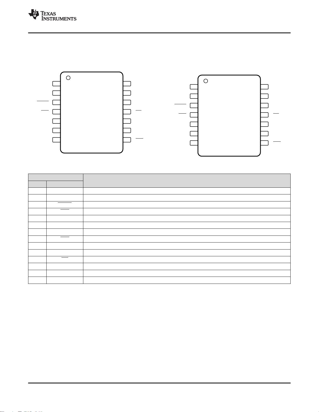
5 Pin Configuration and Functions......................... 3
6 Specifications......................................................... 4
6.1 Absolute Maximum Ratings ..................................... 4
6.2 ESD Ratings.............................................................. 4
6.3 Recommended Operating Conditions....................... 4
6.4 Thermal Information.................................................. 4
6.5 Electrical Characteristics........................................... 5
6.6 I
2
C Interface Timing Requirements........................... 6
6.7 Switching Characteristics.......................................... 7
6.8 Interrupt and Reset Timing Requirements................ 7
6.9 Typical Characteristics.............................................. 8
7 Parameter Measurement Information .................. 9
8 Detailed Description ............................................ 11
8.1 Overview ................................................................. 11
8.2 Functional Block Diagram ....................................... 11
8.3 Feature Description................................................. 12
8.4 Device Functional Modes........................................ 12
8.5 Programming........................................................... 12
8.6 Register Maps......................................................... 14
9 Application and Implementation ........................ 17
9.1 Application Information............................................ 17
9.2 Typical Application .................................................. 17
10 Power Supply Recommendations ..................... 20
10.1 Power-On Reset Requirements ........................... 20
11 Layout................................................................... 22
11.1 Layout Guidelines ................................................. 22
11.2 Layout Example .................................................... 22
12 器器件件和和文文档档支支持持 ..................................................... 23
12.1 接收文档更新通知 ................................................. 23
12.2 支持资源................................................................ 23
12.3 商标 ....................................................................... 23
12.4 静电放电警告......................................................... 23
12.5 Glossary................................................................ 23
13 机机械械、、封封装装和和可可订订购购信信息息....................................... 23
4 修修订订历历史史记记录录
Changes from Revision A (February 2015) to Revision B Page
• Changed the Pin Configuration images appearance.............................................................................................................. 3
• Changed V
CC
= 3.3 V to V
CC
= 2.5 V in Figure 16 .............................................................................................................. 17
Changes from Original (September 2012) to Revision A Page
• 已添加 添加了
引脚配置和功能
部分、ESD
额定值
表、
特性 说明
部分、
器件功能模式
、
应用和实施
部分、
电源相关
建议
部分、
布局
部分、
器件和文档支持
部分以及
机械、封装和可订购信息
部分 ................................................................. 1
• 已添加 向数据表添加了 D 封装............................................................................................................................................... 1
• Changed Handling Ratings table to ESD Ratings.................................................................................................................. 4
• Added D package to the Thermal Information table. ............................................................................................................. 4
1A0 14 VCC
2A1 13 SDA
3RE SET 12 SCL
4INT0 11 INT
5SD0 10 SC1
6SC0 9 SD1
7GND 8 INT1
No t to scale
1A0 14 VCC
2A1 13 SDA
3RE SET 12 SCL
4INT0 11 INT
5SD0 10 SC1
6SC0 9 SD1
7GND 8 INT1
No t to scale
3
TCA9543A
www.ti.com.cn
ZHCSC97B –MARCH 2014–REVISED NOVEMBER 2019
Copyright © 2014–2019, Texas Instruments Incorporated
5 Pin Configuration and Functions
D Package
SOIC 14 Pins
Top View
PW Package
TSSOP 14 Pins
Top View
(1) V
DPUX
is the pull-up reference voltage for the associated data line. V
DPUM
is the master I
2
C reference voltage while V
DPU0
and V
DPU1
are
the slave channel reference voltages.
Pin Functions
PIN
DESCRIPTION
NO. NAME
1 A0 Address input 0. Connect directly to V
CC
or ground.
2 A1 Address input 1. Connect directly to V
CC
or ground.
3 RESET Active-low reset input. Connect to V
CC
or V
DPUM
(1)
through a pull-up resistor, if not used.
4 INT0 Active-low interrupt input 0. Connect to V
DPU0
(1)
through a pull-up resistor.
5 SD0 Serial data 0. Connect to V
DPU0
(1)
through a pull-up resistor.
6 SC0 Serial clock 0. Connect to V
DPU0
(1)
through a pull-up resistor.
7 GND Ground
8 INT1 Active-low interrupt input 1. Connect to V
DPU1
(1)
through a pull-up resistor.
9 SD1 Serial data 1. Connect to V
DPU1
(1)
through a pull-up resistor.
10 SC1 Serial clock 1. Connect to V
DPU1
(1)
through a pull-up resistor.
11 INT Active-low interrupt output. Connect to V
DPUM
(1)
through a pull-up resistor.
12 SCL Serial clock line. Connect to V
DPUM
(1)
through a pull-up resistor.
13 SDA Serial data line. Connect to V
DPUM
(1)
through a pull-up resistor.
14 VCC Supply power
4
TCA9543A
ZHCSC97B –MARCH 2014–REVISED NOVEMBER 2019
www.ti.com.cn
Copyright © 2014–2019, Texas Instruments Incorporated
(1) Stresses beyond those listed under “absolute maximum ratings” may cause permanent damage to the device. These are stress ratings
only, and functional operation of the device at these or any other conditions beyond those indicated under “recommended operating
conditions” is not implied. Exposure to absolute-maximum-rated conditions for extended periods may affect device reliability.
(2) The input negative-voltage and output voltage ratings may be exceeded if the input and output current ratings are observed.
6 Specifications
6.1 Absolute Maximum Ratings
(1)
over operating free-air temperature range (unless otherwise noted)
MIN MAX UNIT
V
CC
Supply voltage range –0.5 7 V
V
I
Input voltage range
(2)
–0.5 7 V
I
I
Input current ±20 mA
I
O
Output current ±25 mA
Continuous current through VCC ±100 mA
Continuous current through GND ±100 mA
P
tot
Total power dissipation 400 mW
T
A
Operating free-air temperature range –40 85 °C
T
stg
Storage temperature range –60 150 °C
(1) JEDEC document JEP155 states that 500-V HBM allows safe manufacturing with a standard ESD control process.
(2) JEDEC document JEP157 states that 250-V CDM allows safe manufacturing with a standard ESD control process.
6.2 ESD Ratings
VALUE UNIT
V
(ESD)
Electrostatic discharge
Human-body model (HBM), per ANSI/ESDA/JEDEC JS-001
(1)
±4000
V
Charged-device model (CDM), per JEDEC specification JESD22-
C101
(2)
±1500
(1) All unused inputs of the device must be held at V
CC
or GND to ensure proper device operation. Refer to the TI application report,
Implications of Slow or Floating CMOS Inputs, literature number SCBA004.
6.3 Recommended Operating Conditions
(1)
MIN MAX UNIT
V
CC
Supply voltage 1.65 5.5 V
V
IH
High-level input voltage
SCL, SDA 0.7 × V
CC
6
V
A1, A0, INT1, INT0, RESET 0.7 × V
CC
V
CC
+ 0.5
V
IL
Low-level input voltage
SCL, SDA –0.5 0.3 × V
CC
V
A1, A0, INT1, INT0, RESET –0.5 0.3 × V
CC
T
A
Operating free-air temperature –40 85 °C
(1) For more information about traditional and new thermal metrics, see the Semiconductor and IC Package Thermal Metrics application
report.
6.4 Thermal Information
THERMAL METRIC
(1)
TCA9543A
UNITPW D
14 PINS 14 PINS
R
θJA
Junction-to-ambient thermal resistance 130.9 102.8
°C/W
R
θJCtop
Junction-to-case (top) thermal resistance 59.2 63.9
R
θJB
Junction-to-board thermal resistance 72.7 57.1
ψ
JT
Junction-to-top characterization parameter 10.5 26.7
ψ
JB
Junction-to-board characterization parameter 72.1 56.8
5
TCA9543A
www.ti.com.cn
ZHCSC97B –MARCH 2014–REVISED NOVEMBER 2019
Copyright © 2014–2019, Texas Instruments Incorporated
(1) For operation between specified voltage ranges, refer to the worst-case parameter in both applicable ranges.
(2) All typical values are at nominal supply voltage (1.8-V, 2.5-V, 3.3-V, or 5-V V
CC
), T
A
= 25°C.
(3) RESET = V
CC
(held high) when all other input voltages, V
I
= GND
(4) The power-on reset circuit resets the I
2
C bus logic when V
CC
< V
PORF
.
6.5 Electrical Characteristics
(1)
over recommended operating free-air temperature range (unless otherwise noted)
PARAMETER TEST CONDITIONS V
CC
MIN TYP
(2)
MAX UNIT
V
PORR
Power-on reset voltage,
VCC rising
No load: V
I
= V
CC
or GND
(3)
1.2 1.5 V
V
PORF
Power-on reset voltage,
VCC falling
(4)
No load: V
I
= V
CC
or GND
(3)
0.8 1 V
V
pass
Switch output voltage
V
SWin
= V
CC
,
I
SWout
= –100 μA
5 V 3.6
V
4.5 V to 5.5 V 2.6 4.5
3.3 V 1.9
3 V to 3.6 V 1.6 2.8
2.5 V 1.4
2.3 V to 2.7 V 1.0 1.8
1.8 V 0.8
1.65 V to 1.95 V 0.5 1.1
I
OH
INT V
O
= V
CC
1.65 V to 5.5 V 10 μA
I
OL
SDA
V
OL
= 0.4 V
1.65 V to 5.5 V
3 7
mAV
OL
= 0.6 V 6 10
INT V
OL
= 0.4 V 3
I
I
SCL, SDA V
I
= V
CC
or GND
(3)
1.65 V to 5.5 V –1 1
μA
SC1–SC0, SD1–SD0 V
I
= V
CC
or GND
(3)
1.65 V to 5.5 V –1 1
A1, A0 V
I
= V
CC
or GND
(3)
1.65 V to 5.5 V –1 1
INT1–INT0 V
I
= V
CC
or GND
(3)
1.65 V to 5.5 V –1 1
RESET V
I
= V
CC
or GND
(3)
1.65 V to 5.5 V –1 1
I
CC
Operating
mode
f
SCL
= 400
kHz
V
I
= V
CC
or GND
(3)
I
O
= 0
t
r,max
= 300 ns
5.5 V 50
μA
3.6 V 20
2.7 V 11
1.65 V 6
f
SCL
= 100
kHz
V
I
= V
CC
or GND
(3)
I
O
= 0
t
r,max
= 1 µs
5.5 V 35
3.6 V 14
2.7 V 5
1.65 V 2
Standby
mode
Low inputs
V
I
= GND
(3)
I
O
= 0
5.5 V 1.6 2
3.6 V 1.0 1.3
2.7 V 0.7 1.1
1.65 V 0.4 0.55
High inputs
V
I
= V
CC
I
O
= 0
5.5 V 1.6 2
3.6 V 1.0 1.3
2.7 V 0.7 1.1
1.65 V 0.4 0.55
ΔI
CC
Supply-
current
change
INT1–INT0
One INT1–INT0 input at 0.6 V,
Other inputs at V
CC
or GND
(3)
1.65 V to 5.5 V
3 20
μA
One INT1–INT0 input at V
CC
– 0.6 V,
Other inputs at V
CC
or GND
(3)
3 20
SCL, SDA
SCL or SDA input at 0.6 V,
Other inputs at V
CC
or GND
(3)
2 15
SCL or SDA input at V
CC
– 0.6 V,
Other inputs at V
CC
or GND
(3)
2 15
剩余32页未读,继续阅读
资源评论
不觉明了
- 粉丝: 3081
- 资源: 5252
上传资源 快速赚钱
- 我的内容管理 展开
- 我的资源 快来上传第一个资源
- 我的收益 登录查看自己的收益
- 我的积分 登录查看自己的积分
- 我的C币 登录后查看C币余额
- 我的收藏
- 我的下载
- 下载帮助
安全验证
文档复制为VIP权益,开通VIP直接复制
信息提交成功