TPD5S116
www.ti.com.cn
ZHCSAK4A –DECEMBER 2012–REVISED MARCH 2013
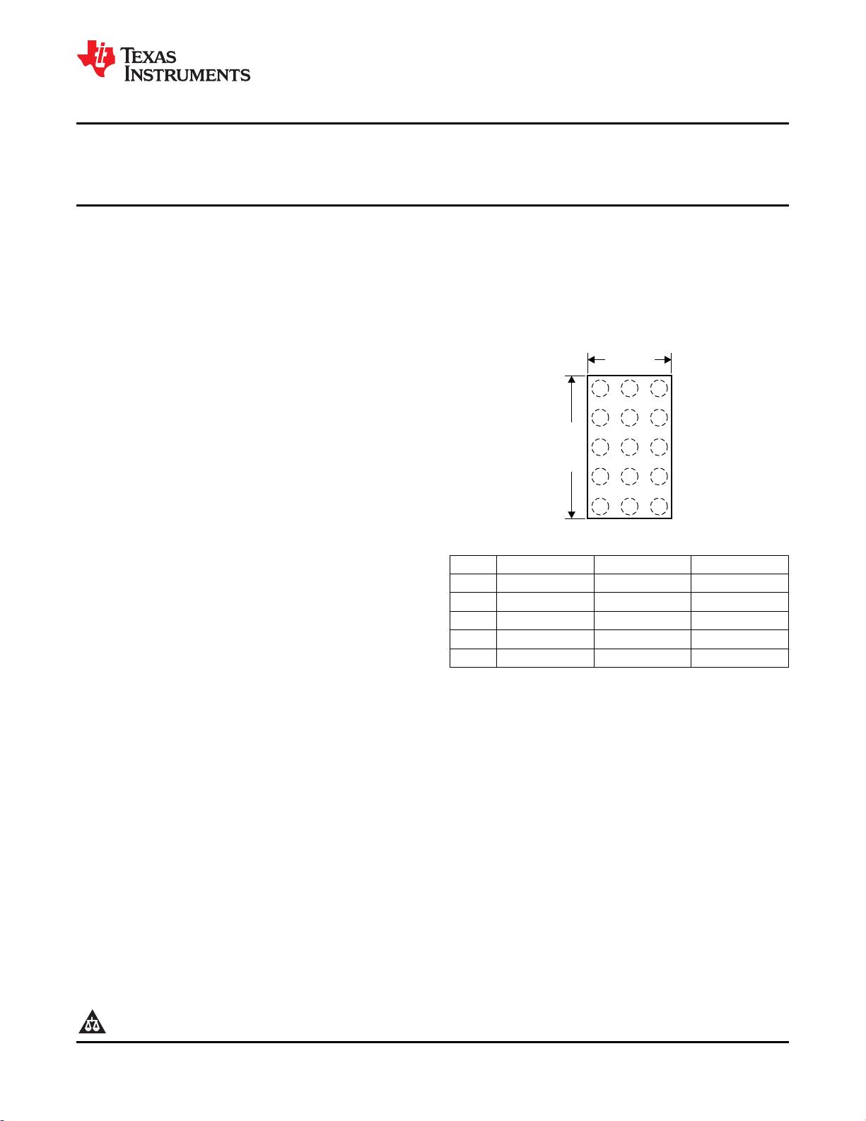
TERMINAL FUNCTIONS
PIN PIN
YFF DESCRIPTION
NAME TYPE
HDMI system side: Hot plug detect Output referenced to VCCA. Connect to
HPD_SYS E1 Output
HDMI controller Hot plug detect input pin
HDMI connector side: Hot plug detect Input. Connect directly to HDMI
HPD_CON E3 Input
Connector Hot Plug Detect pin
HDMI system side CEC signal pin referenced to VCCA. Connect to HDMI
CEC_SYS A1 IO Port
controller.
HDMI connector side CEC signal pin referenced to internal 3.3V supply.
CEC_CON A3 IO Port
Connect to HDMI connector CEC pin.
HDMI system side SCL signal pin referenced to VCCA. Connect to HDMI
SCL_SYS B1 IO Port
controller.
HDMI connector side SCL signal pin referenced to 5V_CON supply. Connect
SCL_CON B3 IO Port
to HDMI connector SCL pin.
HDMI system side SDA signal pin referenced to VCCA. Connect to HDMI
SDA_SYS C1 IO Port
controller.
HDMI connector side SDA signal pin referenced to 5V_CON supply.
SDA_CON C3 IO Port
Connect to HDMI connector SDA pin.
Disables the load switch and HPD when EN =L. The EN pin is referenced to
EN C2 Control Input
VCCA
UTI_CON E2 IO Port Protects the HDMI connector's utility pin
5V_SYS D1 Input Power System side PCB 5V supply; input of load switch
Internal PCB Low Voltage Supply (Same as the HDMI Controller Chip
VCCA A2 Input Supply
Supply)
5V_CON D3 Output Power HDMI connector side external 5V Supply; output of load switch
GND B2, D2 Ground Connect to System Ground Plane
ABSOLUTE MAXIMUM RATINGS
(1)
over operating free-air temperature range (unless otherwise noted)
PARAMETER MIN MAX UNIT
V
CCA
Supply voltage range –0.3 6.0 V
5V_SYS Supply voltage range –0.3 6.0 V
V
I
SCL_SYS, SDA_SYS, CEC_SYS,
–0.3 6.0
EN
Input voltage range
(2)
V
SCL_CON, SDA_CON, CEC_CON,
–0.3 6.0
HPD_CON
V
O
SCL_SYS, SDA_SYS, CEC_SYS,
–0.3 6.0
HPD_SYS
Voltage range applied to any output in the high-
V
impedance or power-off state
(2)(3)
SCL_CON, SDA_CON, CEC_CON,
–0.3 6.0
HPD_CON
V
O
SCL_SYS, SDA_SYS, V
CCA
+
–0.3
CEC_SYS,HPD_SYS 0.5
Voltage range applied to any output in the high or low
V
state(2)(3)
5V_SYS
SCL_CON, SDA_CON, CEC_CON –0.3
+ 0.5
I
IK
Input clamp current VI < 0 –50 mA
I
OK
Output clamp current VO < 0 –50 mA
Continuous current through 5V_SYS, or GND ±100 mA
T
stg
Storage temperature range –65 150 °C
(1) Stresses above these ratings may cause permanent damage. Exposure to absolute maximum conditions for extended periods may
degrade device reliability. These are stress ratings only, and functional operation of the device at these or any other conditions beyond
those specified is not implied.
(2) The input and output voltage ratings may be exceeded if the input and output clamp-current ratings are observed.
(3) The package thermal impedance is calculated in accordance with JESD 51-7.
Copyright © 2012–2013, Texas Instruments Incorporated 5


 我的内容管理
展开
 我的资源
快来上传第一个资源
 我的收益 登录查看自己的收益
 我的积分
登录查看自己的积分
 我的C币
登录后查看C币余额
 我的收藏
我的收藏  我的下载
我的下载  下载帮助
下载帮助 
 前往需求广场,查看用户热搜

 信息提交成功