没有合适的资源?快使用搜索试试~ 我知道了~
资源推荐
资源详情
资源评论


采用小型封装且具有 ±15kV IEC ESD 保护的 TRSF3232E 3V 至 5.5V
双通道 RS-232 1Mbit/s 线路驱动器和接收器
1 特性
• 由 3V 至 5.5V V
CC
电源供电
• 速率高达 1Mbit/s
• 低电源电流:300μA(典型值)
• 外部电容器:4 × 0.1μF
• 接受 5V 逻辑输入及 3.3V 电源
• 闩锁性能超过 100mA,符合 JESD 78 II 类规范
• 为 RS-232 引脚提供 ESD 保护
– ±15kV 人体放电模型 (HBM)
– ±15kV IEC 61000-4-2 空气间隙放电
– ±8kV IEC 61000-4-2 接触放电
• 采用近似于芯片级塑封的 QFN (3mmx3mm) 封装
(比 SOIC-16 小 85%)
2 应用
• 工业 PC
• 有线网络
• 数据中心和企业级计算
• 电池供电型系统
• PDA
• 笔记本电脑
• 掌上电脑
• 手持设备
3 说明
TRSF3232E 由两个线路驱动器、两个线路接收器和一
个双电荷泵电路组成,具有引脚对引脚(串行端口连接
引脚,包括 GND)±15kV ESD 保护。该器件可在异步
通信控制器和串行端口连接器之间提供电气接口。电荷
泵和四个小型外部电容器支持由 3V 至 5.5V 单电源供
电。TRSF3232E 以高达 1Mbit/s 的数据信号传输速率
运行,驱动器输出压摆率为 14V/μs 至 150V/μs。
器件信息
器件型号 封装
(1)
封装尺寸(标称值)
TRSF3232E
D (SOIC) 9.90mm x 3.91mm
DB (SSOP) 6.20mm x 5.30mm
DW (SOIC) 10.3mm x 7.50mm
PW (TSSOP) 5.00mm x 4.40mm
RGT (VQFN) 3.00mm x 3.00mm
(1) 如需了解所有可用封装,请参阅数据表末尾的可订购产品附
录。
DIN1
5 k
5 k
DIN2
ROUT1
ROUT2
DIN1
DIN2
RIN1
RIN2
14
7
13
8
11
10
12
9
逻辑图(正逻辑)
TRSF3232E
ZHCSLP4B – AUGUST 2007 – REVISED JUNE 2021
本文档旨在为方便起见,提供有关 TI 产品中文版本的信息,以确认产品的概要。有关适用的官方英文版本的最新信息,请访问
www.ti.com,其内容始终优先。TI 不保证翻译的准确性和有效性。在实际设计之前,请务必参考最新版本的英文版本。
English Data Sheet: SLLS825

Table of Contents
1 特性................................................................................... 1
2 应用................................................................................... 1
3 说明................................................................................... 1
4 Revision History.............................................................. 2
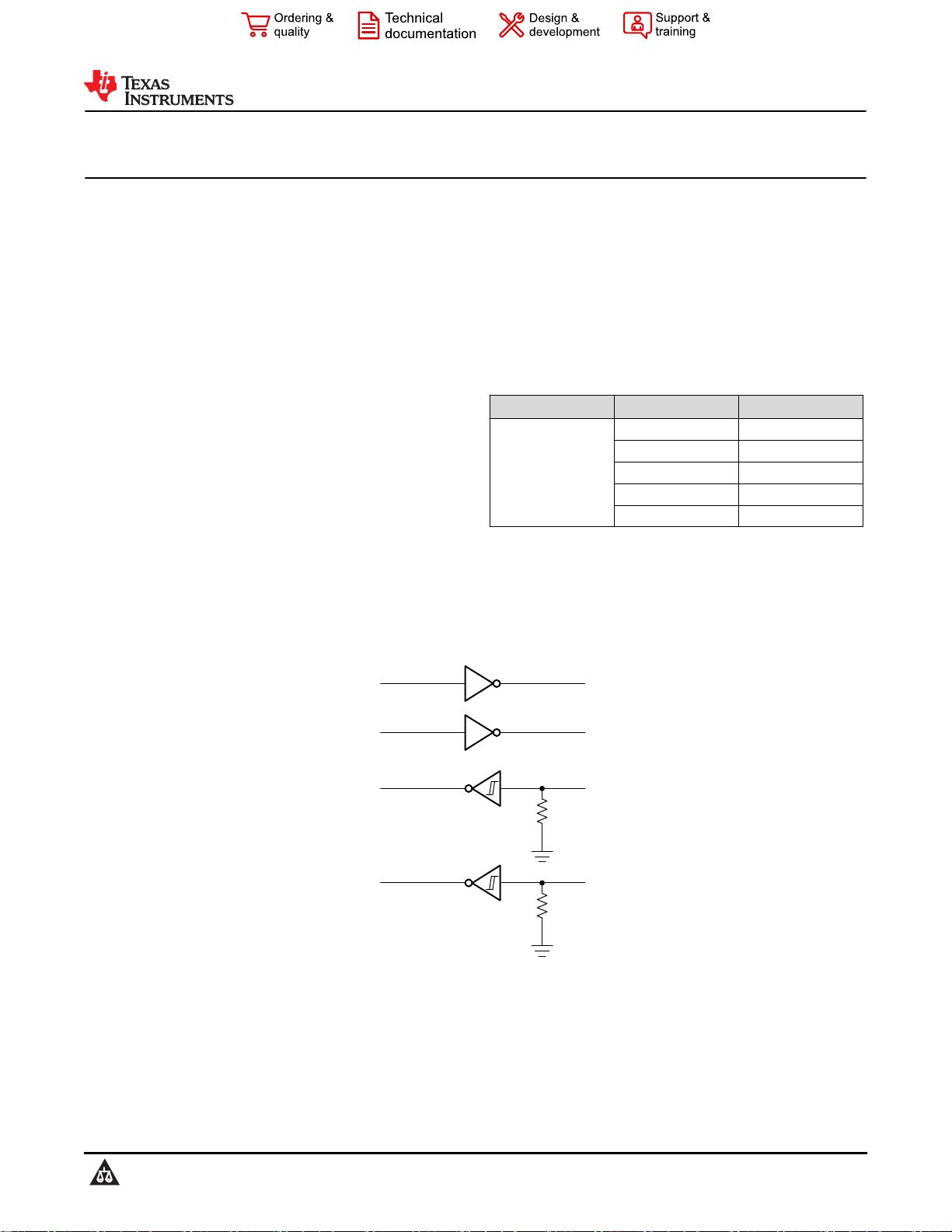
5 Pin Configuration and Functions...................................3
6 Specifications.................................................................. 4
6.1 Absolute Maximum Ratings........................................ 4
6.2 ESD Ratings............................................................... 4
6.3 ESD Protection, Driver................................................4
6.4 ESD Protection, Receiver........................................... 4
6.5 Recommended Operating Conditions.........................5
6.6 Thermal Information....................................................5
6.7 Electrical Characteristics.............................................5
6.8 Electrical Characteristics, Driver................................. 6
6.9 Electrical Characteristics, Receiver............................ 6
6.10 Switching Characteristics, Driver.............................. 7
6.11 Switching Characteristics, Reveiver..........................7
6.12 Typical Characteristics.............................................. 8
7 Parameter Measurement Information............................ 9
8 Detailed Description......................................................10
8.1 Overview................................................................... 10
8.2 Functional Block Diagram......................................... 10
8.3 Feature Description...................................................10
8.4 Device Functional Modes..........................................11
9 Application and Implementation.................................. 12
9.1 Application Information............................................. 12
9.2 Typical Application.................................................... 12
10 Power Supply Recommendations..............................14
11 Layout........................................................................... 14
11.1 Layout Guidelines................................................... 14
11.2 Layout Example...................................................... 14
12 Device and Documentation Support..........................15
12.1 接收文档更新通知................................................... 15
12.2 支持资源..................................................................15
12.3 Trademarks............................................................. 15
12.4 Electrostatic Discharge Caution..............................15
12.5 Glossary..................................................................15
13 Mechanical, Packaging, and Orderable
Information.................................................................... 15
4 Revision History
注:以前版本的页码可能与当前版本的页码不同
Changes from Revision A (December 2020) to Revision B (June 2021) Page
• 添加了
应用
工业 PC、有线网络、数据中心和企业级计算................................................................................... 1
• Changed the table note in the ESD Protection, Driver table to make it applicable to D and PW packages....... 4
• Changed the table note in the ESD Protection, Reciever table to make it applicable to D and PW packages....
4
• Changed the thermal parameter values for D and PW packages in the Thermal Information table...................5
Changes from Revision * (August 2007) to Revision A (December 2020) Page
• 添加了“器件信息”表、“ESD 等级”表、“特性说明”部分、“器件功能模式”、“应用和实施”部分、
“电源相关建议”部分、“布局”部分、“器件和文档支持”部分以及“机械、封装和可订购信息”部分...... 1
• Added Note to the ESD Protection, Driver .........................................................................................................4
• Added Note to the ESD Protection, Receiver .................................................................................................... 4
• Added t
sk(p)
row for RGT package in the Switching Characteristics, Driver........................................................7
• Added t
PLH
and t
PHL
rows for RGT package in the Switching Characteristics, Reveiver ...................................7
• Added t
sk(p)
row for RGT package in the Switching Characteristics, Reveiver .................................................. 7
TRSF3232E
ZHCSLP4B – AUGUST 2007 – REVISED JUNE 2021
www.ti.com.cn
2 Submit Document Feedback
Copyright © 2021 Texas Instruments Incorporated
Product Folder Links: TRSF3232E

5 Pin Configuration and Functions
1
2
3
4
5
6
7
8
16
15
14
13
12
11
10
9
C1+
V+
C1−
C2+
C2−
V−
DOUT2
RIN2
V
CC
GND
DOUT1
RIN1
ROUT1
DIN1
DIN2
ROUT2
图 5-1. D, DB, DW, or PW Package (Top View)
Thermal Pad
1
2
3
4
5
12
11
10
9
6 7 8
16 15 14 13
C1-
C2+
C2-
V-
DOUT1
RIN1
ROUT1
DIN1
DOUT2 RIN2 ROUT2 DIN2
C1+ V+ V
CC
GND
图 5-2. RGT, VQFN Package (Top View)
表 5-1. Pin Functions
PIN
I/O
(1)
DESCRIPTION
NAME D, DB, DW or PW RGT
C1+ 1 16 - Positive lead of C1 capacitor
V+ 2 15 O Positive charge pump output for storage capacitor only
C1- 3 1 - Negative lead of C1 capacitor
C2+ 4 2 - Positive lead of C2 capacitor
C2- 5 3 - Negative lead of C2 capacitor
V- 6 4 O Negative charge pump output for storage capacitor only
DOUT2 7 5 O RS232 line data output (to remote RS232 system)
RIN2 8 6 I RS232 line data input (from remote RS232 system)
ROUT2 9 7 O Logic data output (to UART)
DIN2 10 8 I Logic data input (from UART)
DIN1 11 9 I Logic data input (from UART)
ROUT1 12 10 O Logic data output (to UART)
RIN1 13 11 I RS232 line data input (from remote RS232 system)
DOUT1 14 12 O RS232 line data output (to remote RS232 system)
GRD 15 13 - Ground
V
CC
16
14
-
Supply Voltage, Connect to external 3-V to 5.5-V power
supply
Thermal Pad -
Thermal Pad
-
Exposed thermal pad. Can be connected to GND or left
floating.
(1) Signal Types: I = Input, O = Output, I/O = Input or Output.
www.ti.com.cn
TRSF3232E
ZHCSLP4B – AUGUST 2007 – REVISED JUNE 2021
Copyright © 2021 Texas Instruments Incorporated
Submit Document Feedback
3
Product Folder Links: TRSF3232E

6 Specifications
6.1 Absolute Maximum Ratings
over operating free-air temperature range (unless otherwise noted) see note
(1)
MIN MAX UNIT
V
CC
Supply voltage range
(2)
–0.3
6 V
V+ Positive-output supply voltage range
(2)
–0.3
7 V
V–
Negative-output supply voltage range
(2)
0.3
–7
V
V+ – V–
Supply voltage difference
(2)
13 V
V
I
Input voltage range
Drivers
–0.3
6
V
Receivers
–25
25
V
O
Output voltage range
Drivers
–13.2
13.2
V
Receivers
–0.3
V
CC
+ 0.3
T
J
Operating virtual junction temperature 150 °C
T
stg
Storage temperature range
–65
150 °C
(1) Stresses beyond those listed under "absolute maximum ratings" may cause permanent damage to the device. These are stress ratings
only, and functional operation of the device at these or any other conditions beyond those indicated under "recommended operating
conditions" is not implied. Exposure to absolute-maximum-rated conditions for extended periods may affect device reliability.
(2) All voltages are with respect to network GND.
6.2 ESD Ratings
VALUE UNIT
V
(ESD)
Electrostatic discharge
Human-body model (HBM), per ANSI/ESDA/JEDEC JS-001
1
. ±3000
V
Charged-device model (CDM), per JEDEC specification JESD22-C101
2
±1500
6.3 ESD Protection, Driver
PIN NAME TEST CONDITIONS TYP UNIT
DOUT1, DOUT2
Human-body model (HBM) ±15
kVIEC 61000-4-2 Air-Gap Discharge
(1)
±15
IEC 61000-4-2 Contact Discharge
(1)
±8
(1) For RGT, D and PW packages only: A minimum of 1-µF capacitor is needed between V
CC
and GND to meet the specified IEC ESD
level .
6.4 ESD Protection, Receiver
PIN NAME TEST CONDITIONS TYP UNIT
RIN1, RIN2
HBM ±15
kVIEC 61000-4-2 Air-Gap Discharge
(1)
±15
IEC 61000-4-2 Contact Discharge
(1)
±8
(1) For RGT, D and PW packages only:A minimum of 1-µF capacitor is needed between V
CC
and GND to meet the specified IEC ESD
level.
TRSF3232E
ZHCSLP4B – AUGUST 2007 – REVISED JUNE 2021
www.ti.com.cn
4 Submit Document Feedback
Copyright © 2021 Texas Instruments Incorporated
Product Folder Links: TRSF3232E

6.5 Recommended Operating Conditions
See note
(1)
MIN NOM MAX UNIT
Supply voltage
V
CC
= 3.3 V 3 3.3 3.6
V
V
CC
= 5 V 4.5 5 5.5
V
IH
Driver high-level input voltage DIN
V
CC
= 3.3 V 2
V
V
CC
= 5 V 2.4
V
IL
Driver low-level input voltage DIN 0.8 V
V
I
Driver input voltage DIN 0 5.5
V
Receiver input voltage
–25
25
T
A
Operating free-air temperature
TRSF3232EI
–40
85
°C
TRSF3232EC 0 70
(1) Test conditions are C1–C4 = 0.1 μF at V
CC
= 3.3 V ± 0.3 V; C1 = 0.047 μF, C2–C4 = 0.33 μF at V
CC
= 5 V ± 0.5 V (see 图 9-1 ).
6.6 Thermal Information
THERMAL METRIC
(1)
TRSF3232E
UNITPW (TSSOP) D (SOIC) DW (SOIC)
DB
(SSOP)
RGT (VQFN)
16 Pins 16 Pins 16 Pins 16 Pins 16 Pins
R
θJA
Junction-to-ambient thermal
resistance
108.2 85.9 57 46 48.8 °C/W
R
θJC(top)
Junction-to-case (bottom)
thermal resistance
39.0 43.1 33.5 36.2 55.8 °C/W
R
θJB
Junction-to-board thermal
resistance
54.4 44.5 37.1 43.8 23.2 °C/W
ψ
JT
Junction-to-top
characterization parameter
3.3 10.1 7.5 4.2 1.7 °C/W
ψ
JB
Junction-to-board
characterization parameter
53.8 44.1 37.1 42.9 23.2 °C/W
R
θJC(bot)
Junction-to-case (bottom)
thermal resistance
N/A N/A N/A N/A 9.0 °C/W
(1) For more information about traditional and new thermal metrics, see the Semiconductor and IC package thermal metrics application
report.
6.7 Electrical Characteristics
over recommended ranges of supply voltage and operating free-air temperature (unless otherwise noted)
PARAMETER TEST CONDITIONS
(1)
MIN TYP
(2)
MAX UNIT
I
CC
Supply current No load, V
CC
= 3.3 V or 5 V 0.3 1 mA
(1) Test conditions are C1–C4 = 0.1 μF at V
CC
= 3.3 V ± 0.3 V; C1 = 0.047 μF, C2–C4 = 0.33 μF at V
CC
= 5 V ± 0.5 V (see 图 9-1).
(2) All typical values are at V
CC
= 3.3 V or V
CC
= 5 V, and T
A
= 25°C.
www.ti.com.cn
TRSF3232E
ZHCSLP4B – AUGUST 2007 – REVISED JUNE 2021
Copyright © 2021 Texas Instruments Incorporated
Submit Document Feedback
5
Product Folder Links: TRSF3232E
剩余33页未读,继续阅读
资源评论

不觉明了
- 粉丝: 701
- 资源: 4046

上传资源 快速赚钱
我的内容管理 收起
我的资源 快来上传第一个资源
我的收益
登录查看自己的收益我的积分 登录查看自己的积分
我的C币 登录后查看C币余额
我的收藏
我的下载
下载帮助

会员权益专享
最新资源
- 很棒的毕业设计、课程设计、练手的java项目-员工工资管理系统(文档+视频+源码齐全).rar
- 很棒的毕业设计、课程设计、练手的java项目-学生选课系统(文档+视频+源码齐全).rar
- 很棒的毕业设计、课程设计、练手的java项目-学生选课成绩信息管理系统(ER图文档+视频+源码齐全).rar
- 很棒的毕业设计、课程设计、练手的java项目-学生信息管理(文档+视频+源码齐全).rar
- 很棒的毕业设计、课程设计、练手的java项目-图书管管理系统(视频+源码齐全).rar
- 很棒的毕业设计、课程设计、练手的java项目-汽车租赁管理系统(详细文档+视频+源码齐全).rar
- 很棒的毕业设计、课程设计、练手的java项目-酒店管理系统(流程图+需求背景数据库+架构说明,视频源码齐全).rar
- 很棒的毕业设计、课程设计、练手的java项目-Oracle飞机订票系统(流程图+需求背景+数据库+架构说明+源码).rar
- 很棒的毕业设计、课程设计、练手的java项目-购物系统项目(文档+视频+源码).rar
- 很棒的毕业设计、课程设计、练手的java项目-电影票购票管理系统(视频+源码).rar
资源上传下载、课程学习等过程中有任何疑问或建议,欢迎提出宝贵意见哦~我们会及时处理!
点击此处反馈


安全验证
文档复制为VIP权益,开通VIP直接复制
