TI-TPA6166A2.pdf
需积分: 5 136 浏览量
2022-12-03
16:24:00
上传
评论 4
收藏 1.41MB PDF 举报

SDA
SCL
IRQ
INR
INL
Class-G
Stereo Headphone
Amplifier
CPVDD CPVSS C1P C1N
RING1
TIP
JACK_SENSE
RING2
SLEEVE
ESD
Prot.
MICVDDVDD
PGND
Mic
Bias
MOUTN
MOUTP
GND1
Switch
Matrix
and
Detection
Circuit
Digital
Interface
and
Control
GND2
SAR
ADC
Product
Folder
Sample &
Buy
Technical
Documents
Tools &
Software
Support &
Community
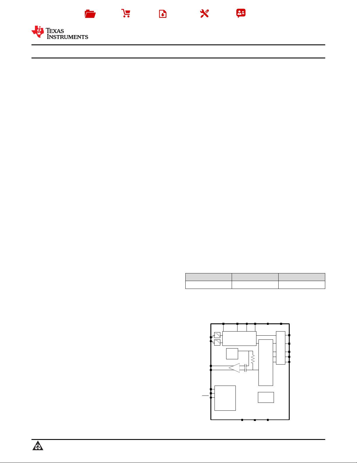
TPA6166A2
SLAS997B –MARCH 2014–REVISED JANUARY 2015
TPA6166A2 3.5-mm Jack Detect and Headset Interface IC
1 Features 3 Description
The TPA6166A2 single-chip headset interface IC
1
• Ultra Low-Power, High-Performance DirectPath™
simplifies the challenges of detecting what kind of
Class-G Headphone Amplifier
device an end user has plugged into the headphone
– Ground-Centered Output Eliminates DC-
jack while delivering excellent audio quality. The
Blocking Capacitors
device enables smaller end products by integrating a
high-performance, low-power DirectPath variable-
– 30 mW/Ch into 32 Ω / Ch at 1% THD+N
attenuation class-G stereo headphone amplifier,
– –42 dB to +6 dB Volume Control
variable-gain microphone preamplifier with bias with
– 2.0 µV Output Noise at –42 dB Gain
advanced accessory detection circuitry, all in a tiny
– 91-dB PSRR 5-mm × 5-mm terminal, 0.4-mm pitch WCSP
package.
– Ground Loop Rejection for Reducing Crosstalk
The class-G headphone amplifier maximizes battery
• Fully Differential Mic Preamplifier With Variable
life by adjusting the supply voltage of the headphone
Gain and 3.4-µV Low Noise
amplifier based on audio signal level. With 8-µV
– Integrated AC-Coupling Capacitor
output noise at 0-dB gain and PSRR of 91 dB, the
– Ground Loop Rejection for Reducing
headphone amplifier provides excellent audio
Headphone to Mic Crosstalk
performance. DirectPath eliminates the need for DC-
blocking capacitors. The microphone preamplifier has
• Choice of Two Mic Bias Voltages: 2.0 V and 2.6 V
two programmable gains of 12 dB and 24 dB, and
– 92-dB PSRR
3.4 µV input referred noise.
– Integrated Programmable Mic Bias Resistor
The microphone bias voltage has two programmable
• Advanced Accessory Insertion, Removal, and
settings of 2 V and 2.6 V. The bias output drives up
Type Detection
to 1.2 mA of current, has a low output noise of 2 µV,
• Passive Multi-button Support Using 10-Bit SAR
and 92-dB PSRR, providing excellent rejection of
ADC power supply noise in wireless handsets.
– Implements Proprietary Scheme to Reduce
The advanced accessory detection algorithm
Error Caused by Audio Playback Signal in
automatically detects six supported accessories and
Presence of Finite Resistance on Headset
enables or disables internal components.
Ground Return Path
Device Information
(1)
• Integrated Level-4 IEC ESD Protection on Jack
PART NUMBER PACKAGE BODY SIZE (NOM)
Connected Pins (on EVM)
TPA6166A2 WSCP (25) 2.50 mm × 2.50 mm
• Ultra Low-Power Chip Shutdown Mode
(1) For all available packages, see the orderable addendum at
• I
2
C Interface
the end of the data sheet.
• Short-Circuit Protection
• 0.4-mm Pitch 25-Ball WCSP
Simplified Schematic
2 Applications
• Smart Phones and Wireless Handsets
• Portable Tablets
• Notebook PCs and Docking Stations
1
An IMPORTANT NOTICE at the end of this data sheet addresses availability, warranty, changes, use in safety-critical applications,
intellectual property matters and other important disclaimers. PRODUCTION DATA.


剩余50页未读,继续阅读
资源评论


