National -54F283.pdf
需积分: 9 112 浏览量
2022-11-29
13:04:04
上传
评论 4
收藏 150KB PDF 举报

TL/F/9513
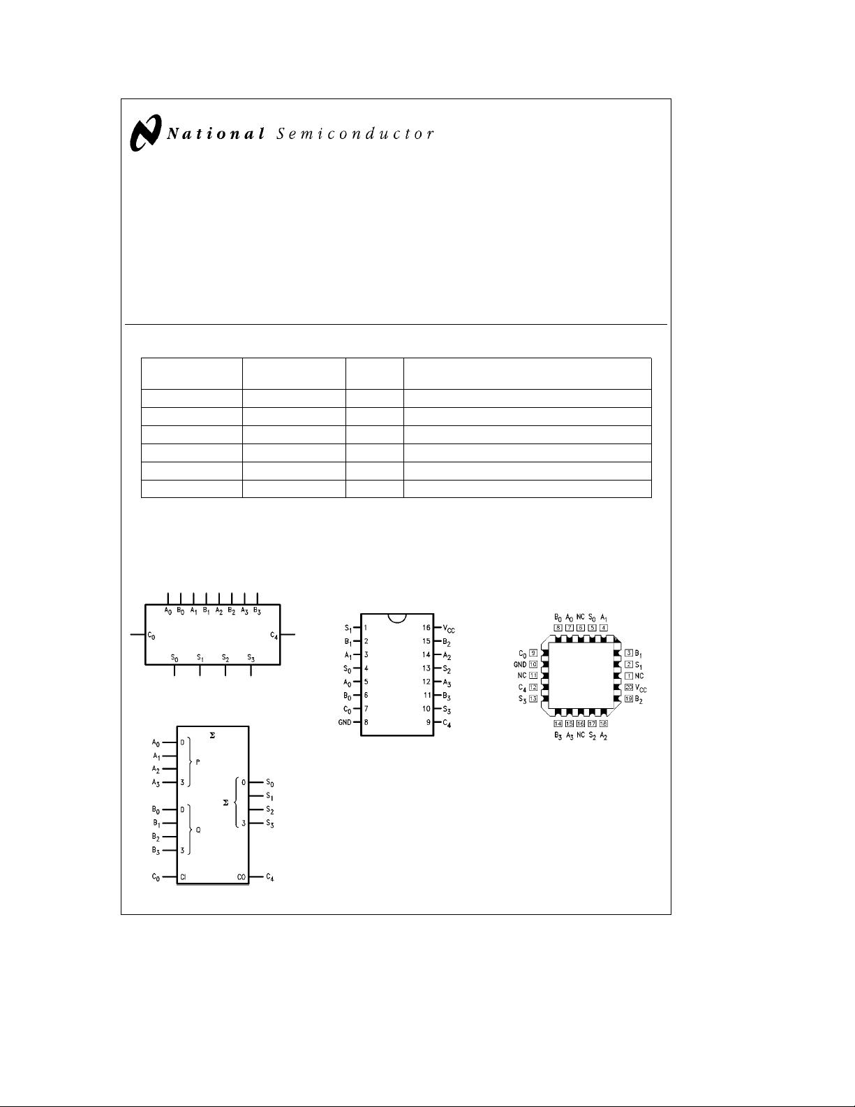
54F/74F283 4-Bit Binary Full Adder with Fast Carry
November 1994
54F/74F283
4-Bit Binary Full Adder with Fast Carry
General Description
The ’F283 high-speed 4-bit binary full adder with internal
carry lookahead accepts two 4-bit binary words (A
0
–A
3
,
B
0
–B
3
) and a Carry input (C
0
). It generates the binary Sum
outputs (S
0
–S
3
) and the Carry output (C
4
) from the most
significant bit. The ’F283 will operate with either active
HIGH or active LOW operands (positive or negative logic).
Features
Y
Guaranteed 4000V minimum ESD protection
Commercial Military
Package
Package Description
Number
74F283PC N16E 16-Lead (0.300
×
Wide) Molded Dual-In-Line
54F283DM (Note 2) J16A 16-Lead Ceramic Dual-In-Line
74F283SC (Note 1) M16A 16-Lead (0.150
×
Wide) Molded Small Outline, JEDEC
74F283SJ (Note 1) M16D 16-Lead (0.300
×
Wide) Molded Small Outline, EIAJ
54F283FM (Note 2) W16A 16-Lead Cerpack
54F283LL (Note 2) E20A 20-Lead Ceramic Leadless Chip Carrier, Type C
Note 1: Devices also available in 13
×
reel. Use suffix
e
SCX and SJX.
Note 2: Military grade device with environmental and burn-in processing. Use suffix
e
DMQB, FMQB and LMQB.
Logic Symbols Connection Diagrams
TL/F/9513–1
IEEE/IEC
TL/F/9513–4
Pin Assignment
for DIP, SOIC and Flatpak
TL/F/9513–2
Pin Assignment
for LCC
TL/F/9513–3
TRI-STATE
É
is a registered trademark of National Semiconductor Corporation.
C
1995 National Semiconductor Corporation RRD-B30M105/Printed in U. S. A.
剩余11页未读,继续阅读
资源评论


