SN54SLC8T245-SEP 8-Bit Dual-Supply Bus Transceiver With Configurable Voltage
Translation and Tri-State Outputs
1 Features
• VID V62/22604
• Radiation tolerant:
– Single event latch-up (SEL) immune up to 43
MeV-cm
2
/mg at 125°C
– Total ionizing dose (TID) Radiation Lot
Acceptance Testing (RLAT) for every wafer lot
up to 20 krad(Si)
• Qualified, fully configurable dual-rail design allows
each port to operate with a power supply range
from 0.65 V to 3.6 V
• Operating temperature from –55°C to +125°C
• Multiple direction-control pins allows simultaneous
up and down translation
• Up to 380 Mbps support when translating from 1.8
V to 3.3 V
• V
CC
isolation feature that effectively isolates both
buses in a power-down scenario
• Partial power-down mode to limit backflow current
in a power-down scenario
• Latch-up performance exceeds 100 mA per JESD
78, class II
• ESD protection exceeds JESD 22
– 8000-V human-body model
– 1000-V charged-device model
2 Applications
• Supports low earth orbit (LEO) space applications
• Space radar and communications
• Space satellite payloads
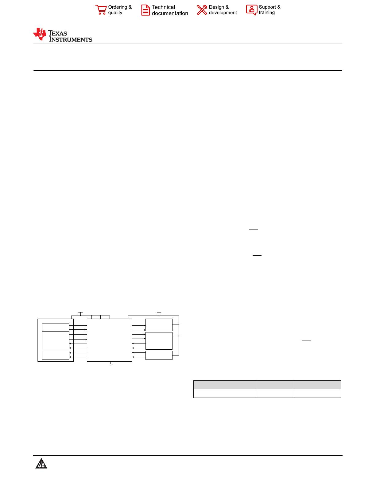
Processor
Interrupts
Control Block
SN54SLC8T245-SEP
A1
A2
A3
A4
A5
A6
A7
A8
B1
B2
B3
B4
B5
B6
B7
B8
Sensor Block
Power Management
Register Map
1.5 V
DIR1 DIR2V
CCA
V
CCB
Data Block
GND
GND
3.3 V
Typical Application Schematic
3 Description
The SN54SLC8T245-SEP device is an 8-bit non-
inverting bus transceiver that resolves voltage level
mismatch between devices operating at the latest
voltage nodes (0.7 V, 0.8 V, and 0.9 V) and devices
operating at industry standard voltage nodes (1.8 V,
2.5 V, and 3.3 V).
The device operates by using two independent power-
supply rails (V
CCA
and V
CCB
) that operate as low as
0.65 V. Data pins A1 through A8 are designed to track
V
CCA
, which accepts any supply voltage from 0.65 V
to 3.6 V. Data pins B1 through B8 are designed to
track V
CCB
, which accepts any supply voltage from
0.65 V to 3.6 V.
The SN54SLC8T245-SEP device is designed for
asynchronous communication between data buses.
The device transmits data from the A bus to the B bus
or from the B bus to the A bus, depending on the logic
level of the direction-control inputs (DIR1 and DIR2).
The output-enable (OE) input is used to disable the
outputs so the buses are effectively isolated.
The SN54SLC8T245-SEP device is designed so the
control pins (DIR and OE) are referenced to V
CCA
.
This device is fully specified for partial-power-down
applications using I
off
. The I
off
circuitry disables
the outputs when the device is powered down.
This inhibits current backflow into the device which
prevents damage to the device.
The V
CC
isolation feature ensures that if either V
CC
input supply is below 100 mV, all level shifter outputs
are disabled and placed into a high-impedance state.
To ensure the high-impedance state of the level shifter
I/Os during power up or power down, OE should be
tied to V
CCA
through a pullup resistor; the minimum
value of the resistor is determined by the current-
sinking capability of the driver.
Device Information
DEVICE NUMBER PACKAGE
(1)
BODY SIZE (NOM)
SN54SLC8T245-SEP TSSOP (24) 4.40 mm × 7.80 mm
(1) For all available packages, see the orderable addendum at
the end of the data sheet.
SN54SLC8T245-SEP
SCES946 – FEBRUARY 2022
An IMPORTANT NOTICE at the end of this data sheet addresses availability, warranty, changes, use in safety-critical applications,
intellectual property matters and other important disclaimers. ADVANCE INFORMATION for preproduction products; subject to change
without notice.


 我的内容管理
展开
 我的资源
快来上传第一个资源
 我的收益 登录查看自己的收益
 我的积分
登录查看自己的积分
 我的C币
登录后查看C币余额
 我的收藏
我的收藏  我的下载
我的下载  下载帮助
下载帮助 
 前往需求广场,查看用户热搜

 信息提交成功