TI-LM140QML.pdf
需积分: 9 24 浏览量
2022-10-28
21:22:11
上传
评论 5
收藏 285KB PDF 举报

LM140QML
www.ti.com
SNVS382B –FEBRUARY 2006–REVISED MAY 2013
LM140QML Three Terminal Positive Regulators
Check for Samples: LM140QML
1
FEATURES
DESCRIPTION
The monolithic 3-terminal positive voltage regulators
2
• Complete Specifications at 1.0A and 0.5A
employ internal current-limiting, thermal shutdown
Loads
and safe-area compensation, making them
• No External Components
essentially indestructible. If adequate heat sinking is
• Internal Thermal Overload Protection
provided, they can deliver over 0.5A output current.
They are intended as fixed voltage regulators in a
• Internal Short Circuit Current-Limiting
wide range of applications including local (on-card)
• Output Transistor Safe-Area Compensation
regulation for elimination of noise and distribution
problems associated with single-point regulation. In
addition to use as fixed voltage regulators, these
devices can be used with external components to
obtain adjustable output voltages and currents.
Considerable effort was expended to make the entire
series of regulators easy to use and minimize the
number of external components. It is not necessary to
bypass the output, although this does improve
transient response. Input bypassing is needed only if
the regulator is located far from the filter capacitor of
the power supply.
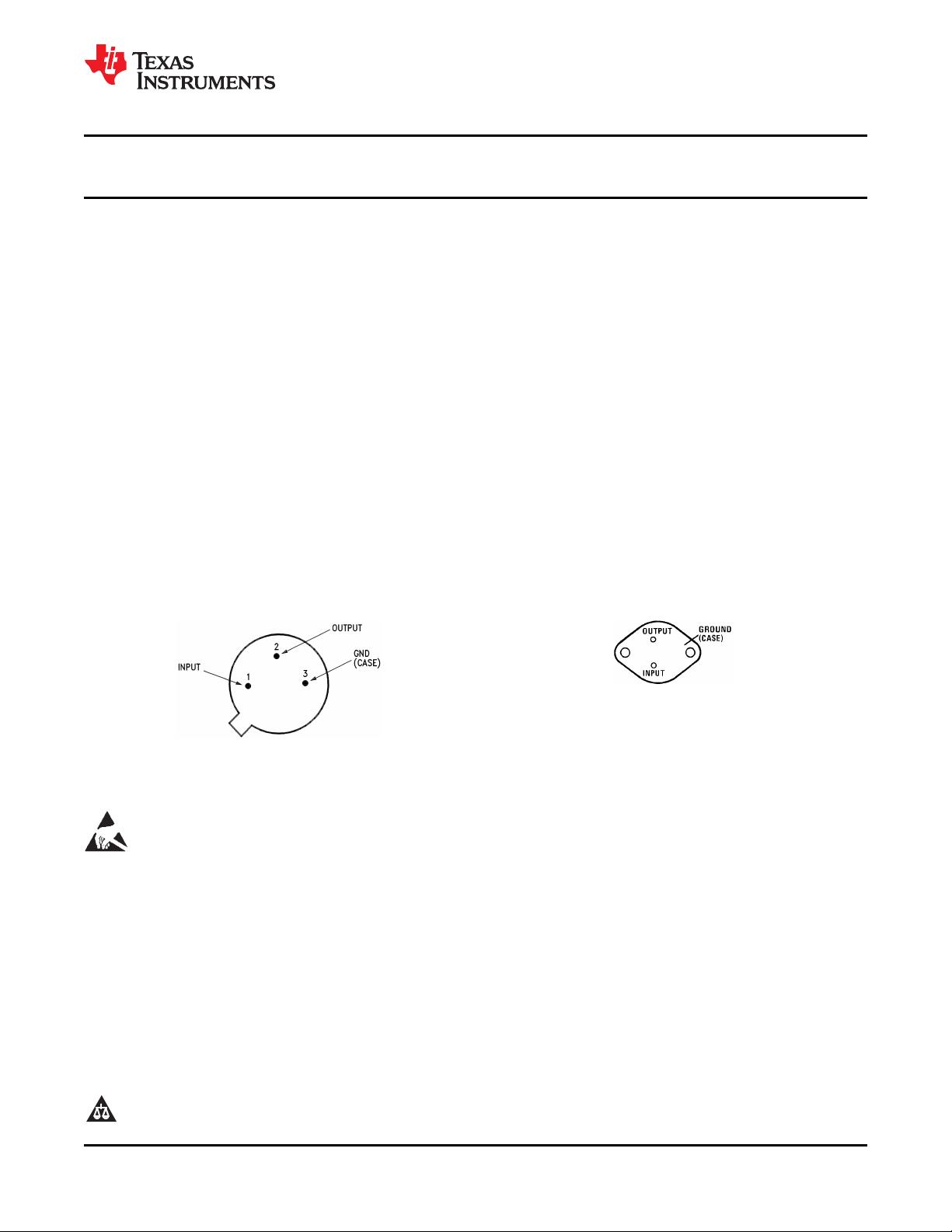
Connection Diagram
Figure 1. Steel Metal Can TO-39 Package (NDT) Figure 2. TO-3 Metal Can (K)
Bottom View Bottom View
See Package Number NDT0003A See Package Number K0002C
These devices have limited built-in ESD protection. The leads should be shorted together or the device placed in conductive foam
during storage or handling to prevent electrostatic damage to the MOS gates.
1
Please be aware that an important notice concerning availability, standard warranty, and use in critical applications of
Texas Instruments semiconductor products and disclaimers thereto appears at the end of this data sheet.
2All trademarks are the property of their respective owners.
PRODUCTION DATA information is current as of publication date.
Copyright © 2006–2013, Texas Instruments Incorporated
Products conform to specifications per the terms of the Texas
Instruments standard warranty. Production processing does not
necessarily include testing of all parameters.

剩余13页未读,继续阅读
资源评论


