TI-LM25183-Q1.pdf
需积分: 13 11 浏览量
2022-10-25
21:45:51
上传
评论 5
收藏 2.17MB PDF 举报

ADVANCEINFORMATION
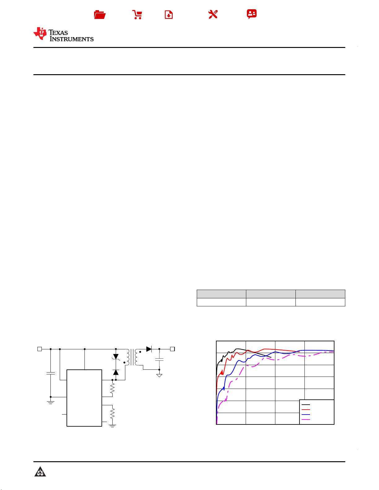
Load Current (mA)
Efficiency (%)
0 200 400 600 800
60
65
70
75
80
85
90
95
D101
V
IN
= 6 V
V
IN
= 12 V
V
IN
= 24 V
V
IN
= 36 V
V
OUT
= 12 V
SW
FB
VIN
EN/UVLO
TC
GND
RSET
LM25183-Q1
C
OUT
C
IN
47 F
10 F
T
1
V
IN
= 4.5 V...42 V
1 : 1
D
FLY
R
FB
124 k:
D
Z
D
F
SS/BIAS
R
SET
12.1 k:
Product
Folder
Order
Now
Technical
Documents
Tools &
Software
Support &
Community
本文档旨在为方便起见,提供有关 TI 产品中文版本的信息,以确认产品的概要。 有关适用的官方英文版本的最新信息,请访问 www.ti.com,其内容始终优先。 TI 不保证翻译的准确
性和有效性。 在实际设计之前,请务必参考最新版本的英文版本。
English Data Sheet: SNVSBJ4
LM25183-Q1
ZHCSL45 –APRIL 2020
具具有有 65V、、2.5A 集集成成MOSFET 的的 LM25183-Q1 42V
IN
PSR 反反激激式式直直流流/直直
流流转转换换器器
1
1 特特性性
1
• 符合AEC-Q100 车规认证
– 器件温度等级 1:-40℃ 至 125℃ 的环境温度范
围
• 提供功能安全
– 可帮助进行功能安全系统设计的可用文档
• 专为可靠耐用的应用 设计
– 4.5V 至 42V 的宽输入电压范围,
– 稳定可靠的解决方案,只有一个组件穿过隔离层
– ±1.5% 的总输出稳压精度
– 可选 V
OUT
温度补偿
– 具有 –40°C 至 +150°C 的结温范围
• 通过集成技术减小解决方案尺寸,降低成本
– 集成 65V、0.11Ω 功率 MOSFET
– 无需光耦合器或变压器辅助绕组即可进行 V
OUT
稳压
• 高效率 PSR 反激运行
– MOSFET 在 BCM 模式下实现准谐振关断
– 具有单输出和多输出实施手段
• 超低的 EMI 传导和辐射信号
– 软开关可避免二极管反向恢复
– 根据标准要求进行了优化CISPR 25 5 类
• 使用 WEBENCH
®
电源设计器创建定制反激式稳压
器设计方案
2 应应用用
• 汽车 HEV/EV 动力总成系统
• AM 以下波段汽车车身电子装置
• 牵引逆变器:IGBT 和 SiC 栅极驱动器电源
3 说说明明
LM25183-Q1 是一款初级侧稳压 (PSR) 反激式转换
器,在 4.5V 至 42V 的宽输入电压范围内具有高效
率。隔离输出电压采样自初级侧反激式电压,因此,无
需使用光耦合器、电压基准或变压器的第三绕组进行输
出电压稳压。高集成度可实现简单可靠的高密度设计,
其中只有一个组件穿过隔离层。通过采用边界导电模式
(BCM) 开关,可实现紧凑的磁解决方案以及优于
±1.5% 的负载和线路调节性能。集成的 65V 功率
MOSFET 可提供高达 10W 的输出功率并提高应对线
路瞬变的余量。
LM25183-Q1 简化了隔离式直流/直流电源的实施,且
可通过可选 功能 优化目标终端设备的性能。该器件通
过一个电阻器来设置输出电压,同时使用可选的电阻器
通过抵消反激式二极管的压降热系数来提高输出电压精
度。其他 特性 包括内部固定或外部可编程软启动、可
实现更高效率的可选偏置电源连接、用于可调节线路
UVLO 的精密使能输入(带迟滞功能)、间断模式过
载保护和带自动恢复功能的热关断保护。
LM25183-Q1 转换器符合汽车 AEC-Q100 1 级标准,
并且采用引脚间距为 0.8mm 且具有可湿性侧面的 8 引
脚 WSON 封装。
器器件件信信息息
(1)
器器件件型型号号 封封装装 封封装装尺尺寸寸((标标称称值值))
LM25183-Q1 WSON (8) 4.00mm × 4.00mm
(1) 如需了解所有可用封装,请参阅数据表末尾的可订购产品附
录。
典典型型应应用用 典典型型效效率率 (V
OUT
= 12V)


剩余40页未读,继续阅读
资源评论


