


Table of Contents
Chapter 1: Introduction.............................................................................................. 4
Features........................................................................................................................................4
IP Facts..........................................................................................................................................5
Chapter 2: Overview......................................................................................................6
Feature Summary........................................................................................................................6
Applications..................................................................................................................................7
Unsupported Features................................................................................................................7
Licensing and Ordering.............................................................................................................. 7
Chapter 3: Product Specification........................................................................... 8
Standards..................................................................................................................................... 8
MIPI D-PHY TX (Master) Core Architecture.............................................................................. 8
MIPI D-PHY RX (Slave) Core Architecture...............................................................................10
MIPI D-PHY Splitter Bridge mode........................................................................................... 12
Performance Resource Use......................................................................................................13
Port Descriptions.......................................................................................................................15
Register Space........................................................................................................................... 24
Chapter 4: Designing with the Core................................................................... 30
General Design Gudelines........................................................................................................30
Shared Logic.............................................................................................................................. 31
I/O Planning...............................................................................................................................36
Clocking...................................................................................................................................... 39
Resets..........................................................................................................................................43
Protocol Description................................................................................................................. 46
Chapter 5: Design Flow Steps.................................................................................56
Customizing and Generating the Core...................................................................................56
Constraining the Core...............................................................................................................64
Simulation.................................................................................................................................. 65
Synthesis and Implementation................................................................................................65
PG202 (v4.2) October 30, 2019 www.xilinx.com
MIPI D-PHY 2
Send Feedback

Chapter 6: Example Design..................................................................................... 66
Overview.....................................................................................................................................66
Simulating the Example Design.............................................................................................. 67
Chapter 7: Test Bench.................................................................................................68
Appendix A: Verification, Compliance, and Interoperability...............70
Hardware Validation................................................................................................................. 70
Appendix B: Debugging.............................................................................................72
Finding Help on Xilinx.com...................................................................................................... 72
Debug Tools............................................................................................................................... 73
Simulation Debug......................................................................................................................74
Hardware Debug.......................................................................................................................75
AXI4-Lite Interface Debug........................................................................................................ 77
Appendix C: Pin and Bank Rules...........................................................................78
Pin Rules for Zynq UltraScale+ MPSoC Devices..................................................................... 78
Pin Rules for 7 series FPGAs.....................................................................................................85
Appendix D: Additional Resources and Legal Notices.............................86
Xilinx Resources.........................................................................................................................86
Documentation Navigator and Design Hubs.........................................................................86
References..................................................................................................................................86
Revision History.........................................................................................................................87
Please Read: Important Legal Notices................................................................................... 89
PG202 (v4.2) October 30, 2019 www.xilinx.com
MIPI D-PHY 3
Send Feedback

Chapter 1
Introduction
The Xilinx
®
MIPI D-PHY Controller is designed for transmission and recepon of video or pixel
data for camera and display interfaces. The core is used as the physical layer for higher level
protocols such as the Mobile Industry Processor Interface (MIPI) Camera Serial Interface (CSI-2)
and Display Serial Interface (DSI).
This product guide provides informaon about using, customizing, and simulang the core for
UltraScale+, and 7 series FPGA families. It also describes the core architecture and provides
details on customizing and interfacing to the core.
Features
• Compliant to MIPI Alliance Standard for D-PHY Specicaon, version 1.2.
• Synchronous transfer at high-speed mode with a bit rate of 80-2500 Mb/s depending on the
device family and speed grade. For details about device family supported line rates see the
UltraScale Architecture SelectIO Resources User Guide (UG571)
• One clock lane and up to four data lanes for TX conguraon.
• One clock lane and up to eight data lanes for RX conguraon.
• Asynchronous transfer at low-power mode with a bit rate of 10 Mb/s.
• Ultra low-power mode, and high-speed mode for clock lane.
• Ultra low-power mode, high-speed mode, and escape mode for data lane.
• PHY-Protocol Interface (PPI) to connect CSI-2 and DSI applicaons.
• Oponal AXI4-Lite interface for register access.
Chapter 1: Introduction
PG202 (v4.2) October 30, 2019 www.xilinx.com
MIPI D-PHY 4
Send Feedback
IP Facts
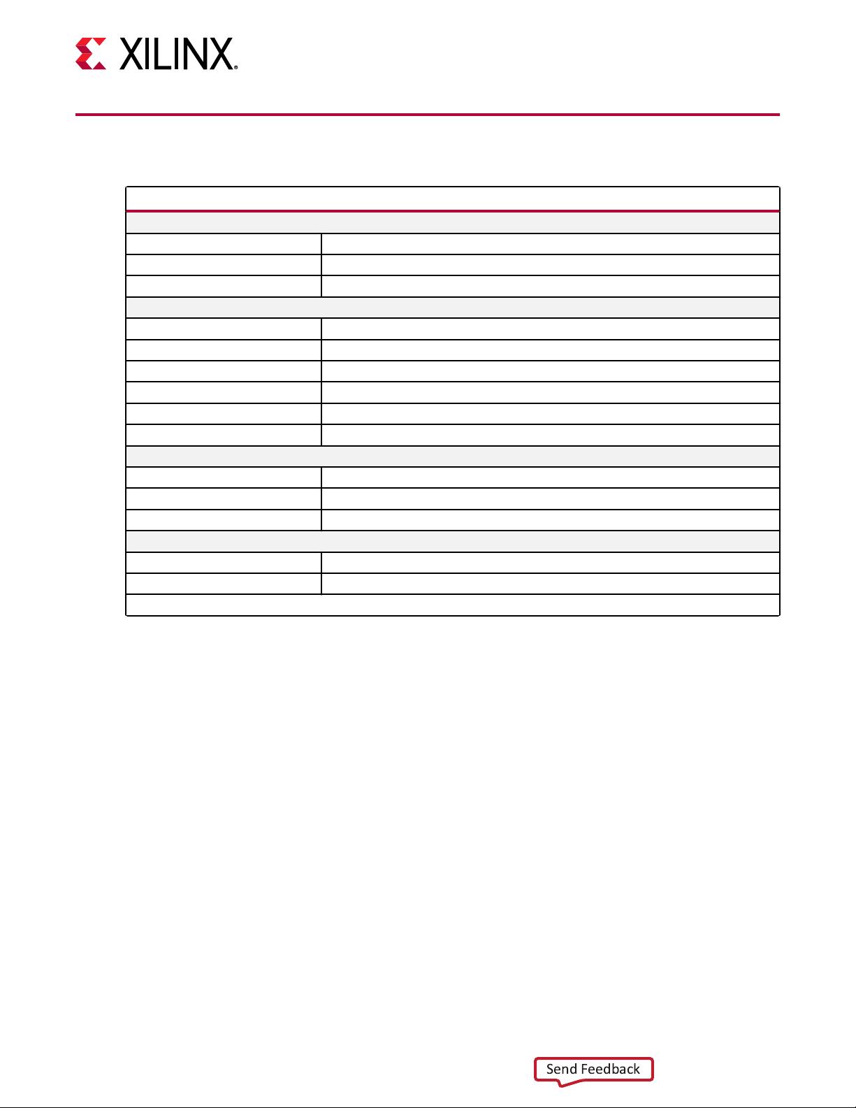
LogiCORE™ IP Facts Table
Core Specifics
Supported Device Family
1
UltraScale+™ Families, Zynq
®
UltraScale+™ MPSoC, Zynq
®
-7000 SoC, 7 series FPGAs
Supported User Interfaces PPI, AXI4-Lite
Resources Performance and Resource Use web page
Provided with Core
Design Files Encrypted RTL
Example Design Verilog
Test Bench Verilog
Constraints File Xilinx Design Contraints (XDC)
Simulation Model Not Provided
Supported S/W Driver N/A
Tested Design Flows
2
Design Entry Vivado
®
Design Suite
Simulation For supported simulators, see the Xilinx Design Tools: Release Notes Guide.
Synthesis Vivado Synthesis
Support
Release Notes and Known Issues Master Answer Records:54550
All Vivado IP Change Logs Master Vivado IP Change Logs: 72775
Provided by Xilinx
®
at the Xilinx Support web page
Notes:
1. For a complete list of supported devices, see the Vivado
®
IP catalog.
2. For the supported versions of the tools, see the Xilinx Design Tools: Release Notes Guide.
Chapter 1: Introduction
PG202 (v4.2) October 30, 2019 www.xilinx.com
MIPI D-PHY 5
Send Feedback


评论6