没有合适的资源?快使用搜索试试~ 我知道了~
本章介绍了基本工作原理,并介绍了SSD应用中使用的浮栅NAND非易失性存储器的主要可靠性和扩展限制。 它进一步讨论了电荷捕获存储器单元作为NAND阵列中浮栅单元的潜在替代,并评估了未来3D存储器方法中两种存储器单元原理的潜力。
资源推荐
资源详情
资源评论
Chapter 5
NAND Flash Technology
M.F. Beug
Abstract This chapter describes the basic operating principle and presents the
major reliability and scaling limitations of floating gate NAND non-volatile memory
as used in SSD applications. It further discusses charge trapping memory cells as
a potential replacement for floating gate cells in the NAND array and evaluates the
potential of both memory cell principles in future 3D memory approaches.
5.1 Flash for SSD Application
Flash memory for non-volatile data storage was introduced commercially in the
mid-1980s. Since then, common ground NOR and NAND architecture have become
the most common memory array architectures. Traditionally, NOR Flash is used for
code storage due to faster memory cell access. NAND Flash is used for mass data
storage as a result of its higher memory density, enabling higher storage capacities.
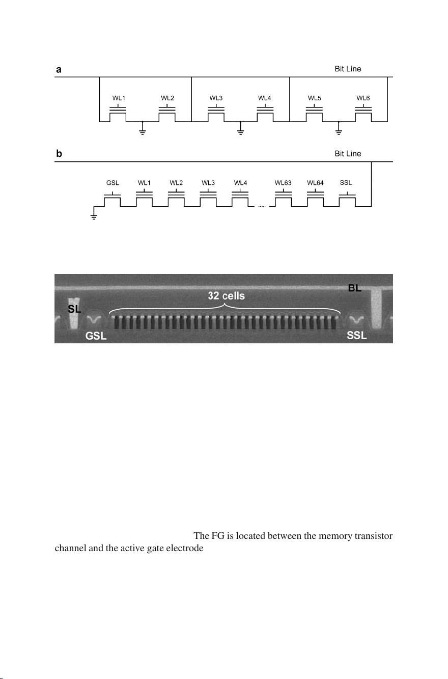
The memory cell area difference can already be seen from the schematic NOR
andNANDarrayimagesinFig.5.1. In the NOR array, two memory cells each
share one contact to ground and one contact to the bit line (see Fig. 5.1a). This
results in an effective memory cell area of about 10 F² (where F is the minimum
feature size). The effective memory cell area of NAND cells is only slightly more
than4F².Figure5.1b shows the so-called NAND string with up to 64 memory cells
connected in a row. To operate the NAND string two additional select transistor
devices (GSL: “Ground Select Line” and SSL: “String Select Line”) and contacts to
ground (SL: “Source Line”) and the bit line (BL) need to be added. These additional
structures cause the effective cell area consumption to be slightly higher than 4 F²
M.F. Beug ()
Physikalisch-Technische Bundesanstalt (PTB), Division 2 “Electricity”, Bundesallee 100,
38116 Braunschweig, Germany
e-mail: Florian.Beug@ptb.de
R. Micheloni et al., Inside Solid State Drives (SSDs), Springer Series
in Advanced Microelectronics 37, DOI 10.1007/978-94-007-5146-0
5,
© Springer ScienceCBusiness Media Dordrecht 2013
79
80 M.F. Beug
Fig. 5.1 Schematic memory cell organization of the NOR array (a) and the NAND array (b). The
word lines (WL) run perpendicular to the bit lines (BL)
Fig. 5.2 SEM picture of a NAND string with 32 cells per string in a 48 nm floating gate NAND
technology [2]
- the theoretically smallest effective cell size. The cross section of a 48 nm NAND
technology with 32 cells per string is shown in Fig. 5.2.
For SSD application, only NAND Flash is a viable option due to the required
high memory capacity and bit cost structure. Therefore, the following sections will
focus on operation, reliability, and scaling topics of NAND Flash.
5.2 Introduction to Floating Gate NAND Operation
A floating gate memory cell stores information in terms of charge in an isolated
gate electrode (floating gate: FG). The FG is located between the memory transistor
channel and the active gate electrode (control gate: CG). This data storage principle
was proposed by Kang and Sze in 1967 [1] and enables data to be stored without
the connection of a supply voltage over time periods of several years.
5 NAND Flash Technology 81
Fig. 5.3 Schematic structure of a floating gate NAND array in word line (WL)(a) and bit line (BL)
direction (b). Corresponding TEM pictures of a 48 nm floating gate NAND technology [2]inWL
direction (c) and BL direction (d)
5.2.1 The Floating Gate NAND Memory Structure
The schematic structure of floating gate NAND cells is shown in Fig. 5.3a, b.
Figure 5.3c, d shows the cross sections of a 48 nm floating gate NAND technology
[2]. The FG and the CG are typically made of polysilicon. For all operations of the
floating gate cell, the active control gate electrode capacitive couples to the floating
gate. The dielectric between the FG and the CG is referred to as inter-poly dielectric
(IPD) and is typically made of a silicon oxide/silicon nitride/silicon oxide triple
layer (ONO). The alterable threshold voltage of a floating gate cell, which represents
the bit information, consequently depends on the coupling strength between the FG
and the CG, and the amount of charge on the FG.
The FG NAND structure in word line direction is shown in Fig. 5.3a, c.
The CG is wrapped around the FG to improve the capacitive coupling from the
CG to the FG. This reduces the operating voltages of the floating gate cells and
ensures a reliable operation as will be described in the next section. The active areas
82 M.F. Beug
(AA) of two neighboring NAND strings are separated by shallow trench insulation
(STI) and are about 200 nm deep in current generations. The memory cell transistor
gate oxide is denoted as tunnel oxide (TOX) because the charge for bit information
storage is transferred through this SiO
2
dielectric by quantum mechanical tunneling.
Generally, it is a very crucial point for reliable floating gate cell operation that
charge during program and erase operations is only transferred through the TOX.
Every charge transfer through the IPD (between FG and CG) needs to be urgently
avoided to prevent severe reliability issues.
In BL direction, the cell strings run as shown in Fig. 5.1a, c and d. The floating
gate cells are patterned by a vertical WL etch step. In the etched spaces between
the floating gate cells, shallow n
C
junctions are implanted in order to define the
memory cell transistors and reduce the string resistance. To improve the charge
retention of the memory cells, the side wall of the floating gate is passivated by a
thermal oxidation process.
The generated high quality thermal side wall oxide (SWOX) forms an effective
tunnel barrier against charge loss from the FG. Subsequently, the space between the
FG cells is filled with a deposited silicon oxide (inter-word line dielectric: IWD)
which generally has a reduced electrical quality. The select devices (GSL and SSL)
are processed together with the floating gate cells and consequently use the TOX
as the gate dielectric. The select transistor gate length is typically in the range of
150–200 nm. To obtain a real transistor for the select devices, the word line layer
is connected to the floating gate layer. This contact is made by removing the ONO
IPD in the middle of the select transistors prior to the CG poly-Si deposition (see
Fig. 5.3d).
The complete process of a floating gate NAND technology is typically based on
30–40 lithographic mask steps and includes 2 poly-Si and 3 metal levels. To obtain
the highest memory density in each technology generation, typically 3 levels are
structured in the most advanced technology node. The levels of advanced feature
size are active area/STI, word line and bit line. The bit line is either done in the first
or second metal layer. There are some more process steps with stringent lithographic
requirements, such as the contacts to the bit line, but also the source contacts, the
CG to FG contacts in the select devices, and others.
5.2.2 The Floating Gate Cell Capacitive Coupling Model
It was described that floating gate NAND cells are arranged in strings with up to 64
memory cells in actual NAND technologies. However for the basic understanding
of the floating gate cell functionality it is necessary to look at a single FG cell first.
Since the floating gate is isolated from the active control gate, all voltages for
operation of the memory cell need to be capacitively coupled to the floating gate. In
principle, the floating gate cell forms a capacitive voltage divider which is typically
described with the aid of the FG cell capacitive coupling model [3]asshownin
Fig. 5.4.
5 NAND Flash Technology 83
V
CG
V
S
V
D
V
B
ψ
s
V
FG
, Q
FG
C
CG
C
S
C
TOX
C
D
C
Si
B
Fig. 5.4 Capacitance model
of a floating gate memory
device
It describes the voltage of the floating gate as a function of the other terminals of
a FG cell. These terminals are typically source (V
S
), drain (V
D
), the bulk terminal
(V
B
), the control gate (V
CG
), and a number of other (parasitic) terminals. All these
terminal voltages are capacitive coupled to the floating gate. The floating gate
voltage can be written as
V
FG
D ˛
G
V
CG
C ˛
S
V
S
C ˛
D
V
D
C
TOX
C
T
§
S
C
Q
FG
C
T
C
X
˛
other
V
other
:
(5.1)
The gate coupling ratio ’
G
in Eq. (5.1) is an important factor and is defined as
˛
G
D
C
CG
C
T
:
(5.2)
C
T
is the total capacitance and is given by
C
T
D C
CG
C C
TOX
C C
S
C C
D
C
P
C
other
:
(5.3)
The sum of C
other
contains all other terminals which couple to a specific floating
gate and represent neighboring bit and word lines or neighboring floating gates.
The capacitive components in the sum are traditionally small compared to the other
terms, but gain significantly in importance when floating gate cells are scaled to
feature sizes below 50 nm [4].
The gate coupling ratio ’
G
describes the portion of the voltage applied between
the CG and the channel that drops across the TOX. For grounded source, drain, bulk,
and other terminals during program operation, the floating gate voltage is given by
V
FG
D ˛
G
V
CG
:
(5.4)
A control gate voltage V
CG
D 20 V in combination with a gate coupling ratio
of ’
G
D 0.6 results in a voltage drop of V
FG
D 12 V across the tunnel oxide.
Consequently, the CG voltage is concentrated on the tunnel oxide, when a high
C
CG
to C
T
ratio and therefore a high ’
G
can be realized.
剩余47页未读,继续阅读
资源评论
weixin_38647517
- 粉丝: 2
- 资源: 965
上传资源 快速赚钱
- 我的内容管理 展开
- 我的资源 快来上传第一个资源
- 我的收益 登录查看自己的收益
- 我的积分 登录查看自己的积分
- 我的C币 登录后查看C币余额
- 我的收藏
- 我的下载
- 下载帮助
安全验证
文档复制为VIP权益,开通VIP直接复制
信息提交成功