没有合适的资源?快使用搜索试试~ 我知道了~
c8015f930中文资料
需积分: 0 0 下载量 84 浏览量
2009-10-17
22:26:11
上传
评论
收藏 4.46MB PDF 举报
温馨提示
试读
320页
c8015f930中文资料 c8015f930的中文资料引脚图
资源详情
资源评论
资源推荐
Single/Dual Battery, 0.9–3.6 V, 64/32 kB, smaRTClock, 10-Bit ADC MCU
C8051F93x-C8051F92x
Rev. 1.0 11/08 Copyright © 2008 by Silicon Laboratories C8051F93x-C8051F92x
Supply Voltage 0.9 to 3.6 V
-
One-Cell Mode supports 0.9 to 1.8 V operation
- Two-Cell Mode supports 1.8 to 3.6 V operation
- Built-in dc-dc converter with 1.8 to 3.3 V output for
use in one-cell mode
- Built-in LDO regulator allows a high analog supply
voltage and low digital core voltage
- 2 built in supply monitors (brownout detectors)
10-Bit Analog to Digital Converter
- ±1 LSB INL; no missing codes
- Programmable throughput up to 300 ksps
- Up to 23 external inputs
- On-Chip Voltage Reference
- On-Chip PGA allows measuring voltages up to twice
the reference voltage.
- 16-bit Auto-Averaging Accumulator with Burst Mode
provides increased ADC resolution.
- Data dependent windowed interrupt generator
- Built-in temperature sensor
Two Comparators
-
Programmable hysteresis and response time
- Configurable as wake-up or reset source
- Up to 23 Capacitive Touch Sense Inputs
6-Bit Programmable Current Reference
-
Up to ±500 µA. Can be used as a bias or for
generating a custom reference voltage.
On-Chip Debug
-
On-chip debug circuitry facilitates full-speed, non-
intrusive in-system debug (No emulator required)
- Provides breakpoints, single stepping
- Inspect/modify memory and registers
- Complete development kit
High-Speed 8051 µC Core
-
Pipelined instruction architecture; executes 70% of
instructions in 1 or 2 system clocks
- Up to 25 MIPS throughput with 25 MHz clock
- Expanded interrupt handler
Memory
-
4352 bytes internal data RAM (256 + 4096)
- 64 kB (‘F93x) or 32 kB (‘F92x) Flash; In-system pro-
grammable in 1024-byte sectors—1024 bytes are
reserved in the
64 kB devices
Digital Peripherals
-
24 or 16 port I/O; All 5 V tolerant with high sink
current and programmable drive strength-Hard
ware
SMBus™ (I
2
C™ Compatible), 2 x SPI™, and UART
serial ports available concurrently
- Four general purpose 16-bit counter/timers
- Programmable 16-bit counter/timer array with six
capture/compare modules and watchdog timer
- Hardware smaRTClock operates down to 0.9 V and
requires less than 0.5 µA supply current.
Clock Sources
-
Internal oscillators: 24.5 MHz, 2% accuracy
supports UART operation; 20 MHz low power
oscill
ator requires very little bias current.
- External oscillator: Crystal, RC, C, or CMOS Clock
- smaRTClock oscillator: 32 kHz Crystal or internal
- Can switch between clock sources on-the-fly; useful
in implementing various power saving modes
Packages
-
32-pin QFN (5 x 5 mm)
- 24-pin QFN (4 x 4 mm)
- 32-pin LQFP (7 x 7 mm, easy to hand-solder)
Temperature Range: –40 to +85 °C
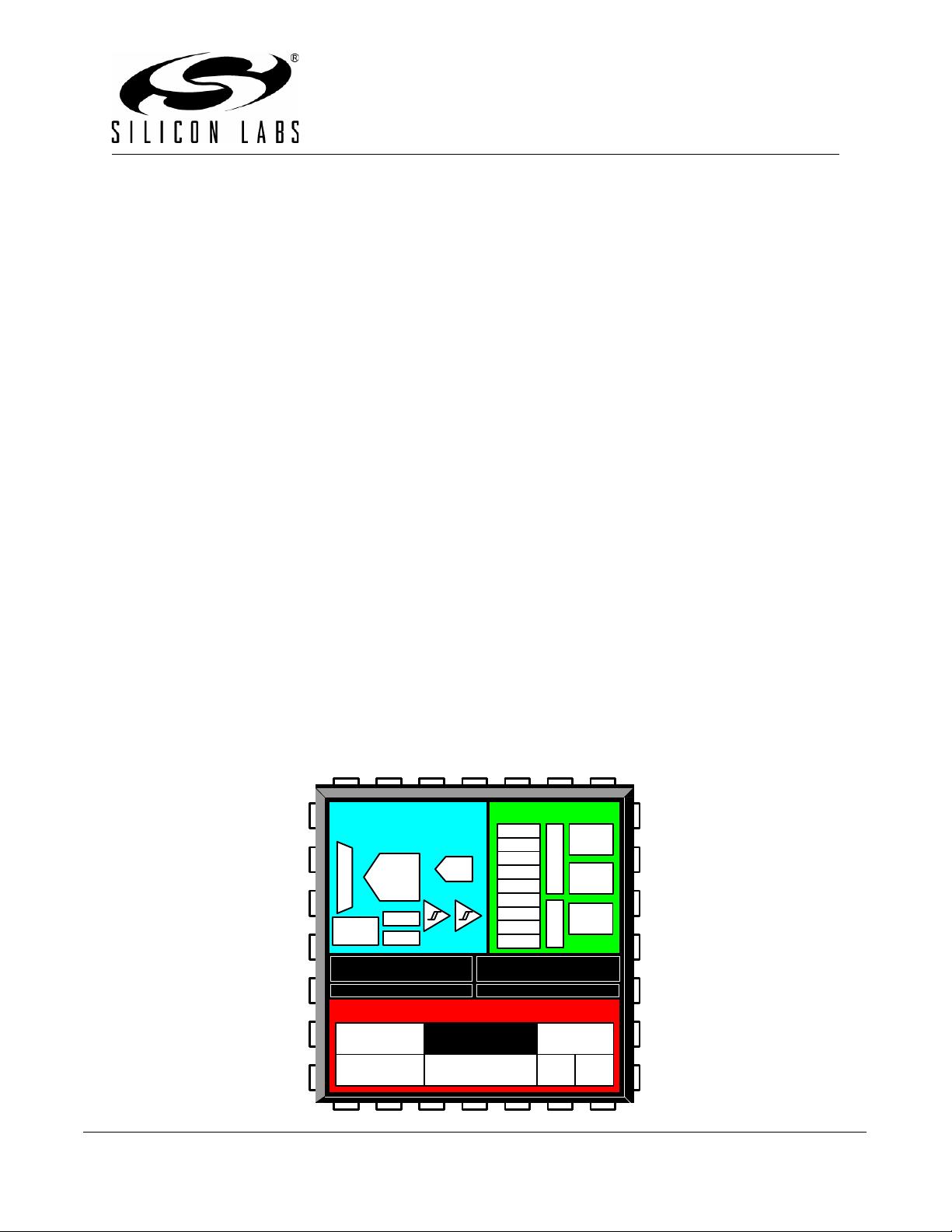
ANALOG
PERIPHERALS
10-bit
300 ksps
ADC
64/32 kB
ISP FLASH
4352 B
SRAM
POR
DEBUG
CIRCUITRY
FLEXIBLE
INTERRUPTS
8051 CPU
(25 MIPS)
TEMP
SENSOR
DIGITAL I/O
24.5 MHz PRECISION
INTERNAL OSCILLATOR
HIGH-SPEED CONTROLLER CORE
A
M
U
X
CROSSBAR
VOLTAGE
COMPARATORS
+
–
WDT
UART
SMBus
PCA
Timer 0
Timer 1
Timer 2
Timer 3
Port 0
2 x SPI
IREF
Port 1
Port 2
+
–
VREG
20 MHz LOW POWER
INTERNAL OSCILLATOR
VREF
CRC
HARDWARE smaRTClockExternal Oscillator
EMIF
C8051F93x-C8051F92x
2 Rev. 1.0
Rev. 1.0 3
C8051F93x-C8051F92x
Table of Contents
1. System Overview.................................................................................................... 18
1.1. CIP-51™ Microcontroller Core.......................................................................... 21
1.1.1. Fully 8051 Compatible.............................................................................. 21
1.1.2. Improved Throughput............................................................................... 21
1.1.3. Additional Features .................................................................................. 21
1.2. Port Input/Output............................................................................................... 22
1.3. Serial Ports ....................................................................................................... 23
1.4. Programmable Counter Array........................................................................... 23
1.5. 10-Bit SAR ADC with 16-bit Auto-Averaging Accumulator and
Autonomous Low Power Burst Mode.................................................................. 24
1.6. Programmable Current Reference (IREF0) ...................................................... 25
1.7. Comparators ..................................................................................................... 25
2. Ordering Information.............................................................................................. 27
3. Pinout and Package Definitions............................................................................ 28
4. Electrical Characteristics....................................................................................... 43
4.1. Absolute Maximum Specifications .................................................................... 43
4.2. Electrical Characteristics................................................................................... 44
5. 10-Bit SAR ADC with 16-bit Auto-Averaging Accumulator and
Autonomous Low Power Burst Mode .................................................................. 60
5.1. Output Code Formatting ................................................................................... 61
5.2. Modes of Operation .......................................................................................... 62
5.2.1. Starting a Conversion............................................................................... 62
5.2.2. Tracking Modes........................................................................................ 63
5.2.3. Burst Mode............................................................................................... 64
5.2.4. Settling Time Requirements..................................................................... 65
5.2.5. Gain Setting.............................................................................................. 66
5.3. 8-Bit Mode......................................................................................................... 66
5.4. Programmable Window Detector...................................................................... 73
5.4.1. Window Detector In Single-Ended Mode ................................................. 75
5.4.2. ADC0 Specifications................................................................................. 75
5.5. ADC0 Analog Multiplexer.................................................................................. 76
5.6. Temperature Sensor......................................................................................... 78
5.6.1. Calibration ................................................................................................ 79
5.7. Voltage and Ground Reference Options........................................................... 81
5.8. External Voltage References ............................................................................
82
5.9. Internal Voltage References ............................................................................. 82
5.10.Analog Ground Reference................................................................................ 82
5.11.Temperature Sensor Enable ............................................................................ 83
5.12.Voltage Reference Electrical Specifications..................................................... 84
6. Programmable Current Reference (IREF0) .......................................................... 85
6.1. IREF0 Specifications......................................................................................... 85
7. Comparators ........................................................................................................... 86
7.1. Comparator Inputs ............................................................................................ 86
C8051F93x-C8051F92x
4 Rev. 1.0
7.2. Comparator Outputs ......................................................................................... 87
7.3. Comparator Response Time............................................................................. 88
7.4. Comparator Hysterisis ...................................................................................... 88
7.5. Comparator Register Descriptions.................................................................... 89
7.6. Comparator0 and Comparator1 Analog Multiplexers........................................ 93
8. CIP-51 Microcontroller ........................................................................................... 96
8.1. Instruction Set................................................................................................... 97
8.1.1. Instruction and CPU Timing ..................................................................... 97
8.2. CIP-51 Register Descriptions.......................................................................... 102
9. Memory Organization........................................................................................... 105
9.1. Program Memory ............................................................................................ 106
9.1.1. MOVX Instruction and Program Memory ............................................... 106
9.2. Data Memory .................................................................................................. 107
9.2.1. Internal RAM .......................................................................................... 107
9.2.2. External RAM ......................................................................................... 108
10.External Data Memory Interface and On-Chip XRAM........................................ 109
10.1.Accessing XRAM............................................................................................ 109
10.1.1.16-Bit MOVX Example ........................................................................... 109
10.1.2.8-Bit MOVX Example ............................................................................. 109
10.2.Configuring the External Memory Interface for Off-Chip Access.................... 110
10.3.External Memory Interface Port Input/Output Configuration........................... 110
10.4.Multiplexed External Memory Interface .......................................................... 111
10.5.External Memory Interface Operating Modes................................................. 113
10.5.1.Internal XRAM Only ............................................................................... 113
10.5.2.Split Mode without Bank Select.............................................................. 113
10.5.3.Split Mode with Bank Select................................................................... 114
10.5.4.External Only.......................................................................................... 114
10.6.External Memory Interface Timing.................................................................. 114
10.7.EMIF Special Function Registers ................................................................... 115
10.8.EMIF Timing Diagrams................................................................................... 118
10.8.1.Multiplexed 16-bit MOVX: EMI0CF[3:2] = 01, 10, or 11......................... 118
10.8.2.Multiplexed 8-bit MOVX without Bank Select: EMI0CF[3:2] = 01 or 11. 119
11.Special Function Registers ................................................................................. 122
11.1.SFR Paging .................................................................................................... 123
12.Interrupt Handler .................................................................................................. 129
12.1.Enabling Interrupt Sources............................................................................. 129
12.2.MCU Interrupt Sources and Vectors
............................................................... 129
12.3.Interrupt Priorities ........................................................................................... 130
12.4.Interrupt Latency............................................................................................. 130
12.5.Interrupt Register Descriptions....................................................................... 132
12.6.External Interrupts INT0
and INT1.................................................................. 139
13.Flash Memory ....................................................................................................... 141
13.1.Programming The Flash Memory................................................................... 141
13.1.1.Flash Lock and Key Functions............................................................... 141
13.1.2.Flash Erase Procedure .......................................................................... 142
Rev. 1.0 5
C8051F93x-C8051F92x
13.1.3.Flash Write Procedure ........................................................................... 142
13.2.Non-volatile Data Storage .............................................................................. 143
13.3.Security Options ............................................................................................. 143
13.4.Flash Write and Erase Guidelines.................................................................. 145
13.4.1.VDD Maintenance and the VDD Monitor ............................................... 145
13.4.2.PSWE Maintenance............................................................................... 146
13.4.3.System Clock ......................................................................................... 146
13.5.Minimizing Flash Read Current ...................................................................... 147
14.Power Management.............................................................................................. 151
14.1.Normal Mode.................................................................................................. 152
14.2.Idle Mode........................................................................................................ 153
14.3.Stop Mode ...................................................................................................... 153
14.4.Suspend Mode ............................................................................................... 154
14.5.Sleep Mode .................................................................................................... 154
14.6.Configuring Wakeup Sources......................................................................... 155
14.7.Determining the Event that Caused the Last Wakeup.................................... 155
14.8.Power Management Specifications ................................................................ 157
15.Cyclic Redundancy Check Unit (CRC0) ............................................................. 158
15.1.CRC Algorithm................................................................................................ 158
15.2.Preparing for a CRC Calculation .................................................................... 160
15.3.Performing a CRC Calculation ....................................................................... 160
15.4.Accessing the CRC0 Result ........................................................................... 160
15.5.CRC0 Bit Reverse Feature............................................................................. 164
16.On-Chip DC-DC Converter (DC0) ........................................................................ 165
16.1.Startup Behavior............................................................................................. 166
16.2.Pulse Skipping Mode...................................................................................... 167
16.3.Enabling the DC-DC Converter ...................................................................... 167
16.4.Selecting the Optimum Switch Size................................................................ 168
16.5.DC-DC Converter Clocking Options............................................................... 168
16.6.DC-DC Converter Behavior in Sleep Mode.................................................... 168
16.7.DC-DC Converter Register Descriptions........................................................ 170
16.8.DC-DC Converter Specifications.................................................................... 171
17.Voltage Regulator (VREG0) ................................................................................. 172
17.1.Voltage Regulator Electrical Specifications
.................................................... 172
18.Reset Sources....................................................................................................... 173
18.1.Power-On (VBAT Supply Monitor) Reset ....................................................... 174
18.2.Power-Fail (VDD/DC+ Supply Monitor) Reset................................................ 175
18.3.External Reset................................................................................................ 178
18.4.Missing Clock Detector Reset ........................................................................ 178
18.5.Comparator0 Reset ........................................................................................ 178
18.6.PCA Watchdog Timer Reset .......................................................................... 178
18.7.Flash Error Reset ........................................................................................... 179
18.8.smaRTClock (Real Time Clock) Reset........................................................... 179
18.9.Software Reset............................................................................................... 179
19.Clocking Sources ................................................................................................. 181
剩余319页未读,继续阅读
wangjian6655
- 粉丝: 1
- 资源: 3
上传资源 快速赚钱
- 我的内容管理 展开
- 我的资源 快来上传第一个资源
- 我的收益 登录查看自己的收益
- 我的积分 登录查看自己的积分
- 我的C币 登录后查看C币余额
- 我的收藏
- 我的下载
- 下载帮助
安全验证
文档复制为VIP权益,开通VIP直接复制
信息提交成功
评论0